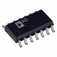
OP484FS Analog Devices Inc, OP484FS Datasheet - Page 17

OP484FS
Manufacturer Part Number
OP484FS
Description
IC OPAMP GP R-R 4.25MHZ 14SOIC
Manufacturer
Analog Devices Inc
Datasheet
1.OP184FSZ.pdf
(24 pages)
Specifications of OP484FS
Slew Rate
4 V/µs
Rohs Status
RoHS non-compliant
Amplifier Type
General Purpose
Number Of Circuits
4
Output Type
Rail-to-Rail
Gain Bandwidth Product
4.25MHz
Current - Input Bias
80nA
Voltage - Input Offset
250µV
Current - Supply
2.25mA
Current - Output / Channel
10mA
Voltage - Supply, Single/dual (±)
3 V ~ 36 V, ±1.5 V ~ 18 V
Operating Temperature
-40°C ~ 125°C
Mounting Type
Surface Mount
Package / Case
14-SOIC (3.9mm Width), 14-SOL
No. Of Amplifiers
4
Bandwidth
4.25MHz
No. Of Pins
14
Peak Reflow Compatible (260 C)
No
Input Bias Current
80nA
Input Offset Voltage Max
0.15mV
Leaded Process Compatible
No
-3db Bandwidth
-
Lead Free Status / RoHS Status
Contains lead / RoHS non-compliant
Available stocks
Company
Part Number
Manufacturer
Quantity
Price
Part Number:
OP484FS
Manufacturer:
ADI/亚德诺
Quantity:
20 000
Part Number:
OP484FSZ
Manufacturer:
ADI/亚德诺
Quantity:
20 000
Company:
Part Number:
OP484FSZ-REEL
Manufacturer:
ST
Quantity:
9 121
Part Number:
OP484FSZ-REEL7
Manufacturer:
ADI/亚德诺
Quantity:
20 000
Resistor networks should be used in this circuit for R2 and R3
because they exhibit the necessary relative tolerance matching for
good performance. Matched networks also exhibit tight relative
resistor temperature coefficients for good circuit temperature
stability. Trimming Potentiometer P1 is used for optimum dc
CMR adjustment, and C1 is used to optimize ac CMR. With the
circuit values as shown, Circuit CMR is better than 80 dB over the
frequency range of 20 Hz to 20 kHz. Circuit referred-to-input
(RTI) noise in the 0.1 Hz to 10 Hz band is an impressively low
0.45 μV p-p. Resistor RP1 and Resistor RP2 serve to protect the
OP284 inputs against input overvoltage abuse. Capacitor C2 can
be included to the limit circuit bandwidth and, therefore, wide
bandwidth noise in sensitive applications. The value of this
capacitor should be adjusted, depending on the required closed-
loop bandwidth of the circuit. The R4 to C2 time constant creates
a pole at a frequency equal to
2.5 V REFERENCE FROM A 3 V SUPPLY
In many single-supply applications, the need for a 2.5 V reference
often arises. Many commercially available monolithic 2.5 V
references require at least a minimum operating supply of 4 V.
The problem is exacerbated when the minimum operating
supply voltage is 3 V. The circuit illustrated in Figure 53 is an
example of a 2.5 V reference that operates from a single 3 V
supply. The circuit takes advantage of the OP284 rail-to-rail
input/output voltage ranges to amplify an
output to 2.5 V.
The low TCV
output voltage temperature coefficient that is dominated by
the temperature coefficients of R2 and R3. In this circuit with
100 ppm/°C TCR resistors, the output voltage exhibits a tempera-
ture coefficient of 200 ppm/°C. Lower tempco resistors are
recommended for more accurate performance over temperature.
5pF TO 40pF
AC CMRR
V
Figure 52. Single Supply, 3 V Low Noise Instrumentation Amplifier
IN
f
( )
TRIM
3
+
–
C1
dB
=
RP1
RP2
1kΩ
1kΩ
OS
2
of the OP284 at 1.5 μV/°C helps maintain an
π
R
1
4
3
2
P1
500Ω
R1
9.53kΩ
C
2
A1
1.1kΩ
SET R2 = R3
A1, A2 = 1/2 OP284
GAIN = 1 +
R2
1
R1 + P1 = R4
1.1kΩ
R4
R3
R3
AD589
5
6
A2
10kΩ
R4
3V
C2
8
4
1.235 V
7
V
OUT
Rev. I | Page 17 of 24
One measure of the performance of a voltage reference is its
capacity to recover from sudden changes in load current. While
sourcing a steady-state load current of 1 mA, this circuit recovers
to 0.01% of the programmed output voltage in 1.5 μs for a total
change in load current of ±1 mA.
5 V ONLY, 12-BIT DAC SWINGS RAIL-TO-RAIL
The OP284 is ideal for use with a CMOS DAC to generate a
digitally controlled voltage with a wide output range. Figure 54
shows a DAC8043 used in conjunction with the AD589 to gen-
erate a voltage output from 0 V to 1.23 V. The DAC is actually
operating in voltage switching mode, where the reference is
connected to the current output, I
taken from the V
as opposed to the classic current output mode, which is inverting
and not usable in single-supply applications.
In this application, the OP284 serves two functions. First, it
buffers the high output impedance of the DAC V
is on the order of 10 kΩ. The op amp provides a low impedance
output to drive any following circuitry.
Second, the op amp amplifies the output signal to provide a rail-
to-rail output swing. In this particular case, the gain is set to 4.1
so that the circuit generates a 5 V output when the DAC output
is at full scale. If other output voltage ranges are needed, such as
0 V ≤ V
the values of R2 and R3.
AD589
17.8kΩ
1.23V
R1
Figure 53. 2.5 V Reference That Operates on a Single 3 V Supply
OUT
3
AD589
17.4kΩ
≤ 4.095 V, the gain can be easily changed by adjusting
Figure 54. 5 V Only, 12-Bit DAC Swings Rail-to-Rail
I
OUT
R1
RESISTORS = 1%, 100ppm/°C
POTENTIOMETER = 10 TURN, 100ppm/°C
+
–
GND CLK SR1 LD
3V
REF
DAC8043
V
4
5V
DD
pin. This topology is inherently noninverting,
100kΩ
8
232Ω
R3
CONTROL
1%
7
R3
DIGITAL
6
32.4Ω
3
2
V
R
R2
1%
REF
RB
1/2
OP284
100kΩ
5
OP184/OP284/OP484
R2
3V
2
1
8
4
OUT
2
3
OP284
, and the output voltage is
100kΩ
1
1/2
5kΩ
1%
R4
P1
5V
0.1µF
8
4
1
2.5V
REF
V
REF
OUT
pin, which
=
4096
D
(5V)


