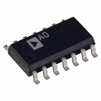
OP484FS Analog Devices Inc, OP484FS Datasheet - Page 18

OP484FS
Manufacturer Part Number
OP484FS
Description
IC OPAMP GP R-R 4.25MHZ 14SOIC
Manufacturer
Analog Devices Inc
Datasheet
1.OP184FSZ.pdf
(24 pages)
Specifications of OP484FS
Slew Rate
4 V/µs
Rohs Status
RoHS non-compliant
Amplifier Type
General Purpose
Number Of Circuits
4
Output Type
Rail-to-Rail
Gain Bandwidth Product
4.25MHz
Current - Input Bias
80nA
Voltage - Input Offset
250µV
Current - Supply
2.25mA
Current - Output / Channel
10mA
Voltage - Supply, Single/dual (±)
3 V ~ 36 V, ±1.5 V ~ 18 V
Operating Temperature
-40°C ~ 125°C
Mounting Type
Surface Mount
Package / Case
14-SOIC (3.9mm Width), 14-SOL
No. Of Amplifiers
4
Bandwidth
4.25MHz
No. Of Pins
14
Peak Reflow Compatible (260 C)
No
Input Bias Current
80nA
Input Offset Voltage Max
0.15mV
Leaded Process Compatible
No
-3db Bandwidth
-
Lead Free Status / RoHS Status
Contains lead / RoHS non-compliant
Available stocks
Company
Part Number
Manufacturer
Quantity
Price
Part Number:
OP484FS
Manufacturer:
ADI/亚德诺
Quantity:
20 000
Part Number:
OP484FSZ
Manufacturer:
ADI/亚德诺
Quantity:
20 000
Company:
Part Number:
OP484FSZ-REEL
Manufacturer:
ST
Quantity:
9 121
Part Number:
OP484FSZ-REEL7
Manufacturer:
ADI/亚德诺
Quantity:
20 000
OP184/OP284/OP484
HIGH-SIDE CURRENT MONITOR
In the design of power supply control circuits, a great deal of design
effort is focused on ensuring the long-term reliability of a pass
transistor over a wide range of load current conditions. As a result,
monitoring and limiting device power dissipation is of prime
importance in these designs. The circuit shown in Figure 55 is
an example of a 3 V, single-supply, high-side current monitor that
can be incorporated into the design of a voltage regulator with
fold-back current limiting or a high current power supply with
crowbar protection. This design uses an OP284 rail-to-rail input
voltage range to sense the voltage drop across a 0.1 Ω current shunt.
A P-channel MOSFET, used as the feedback element in the circuit,
converts the differential input voltage of the op amp into a current.
This current is applied to R2 to generate a voltage that is a linear
representation of the load current. The transfer equation for the
current monitor is given by
For the element values shown, the transfer characteristic of the
monitor output is 2.5 V/A.
CAPACITIVE LOAD DRIVE CAPABILITY
The OP284 exhibits excellent capacitive load driving capabilities.
It can drive up to 1 nF, as shown in Figure 30. Even though the
device is stable, a capacitive load does not come without penalty in
bandwidth. The bandwidth is reduced to less than 1 MHz for loads
greater than 2 nF. A snubber network on the output does not
increase the bandwidth, but it does significantly reduce the amount
of overshoot for a given capacitive load.
A snubber consists of a series R-C network (R
Figure 56, connected from the output of the device to ground.
This network operates in parallel with the load capacitor, C
provide the necessary phase lag compensation. The value of the
resistor and capacitor is best determined empirically.
Monitor Output =
MONITOR
OUTPUT
Figure 55. High-Side Load Current Monitor
3V
SI9433
100Ω
M1
R1
S
R2
D
R
R2
2.49kΩ
×
SENSE
0.1Ω
⎛
⎜
⎝
G
R
SENSE
R1
3
2
1/2
OP284
⎞
⎟
⎠
×
3V
I
4
8
L
0.1µF
I
L
S
1
, C
S
), as shown in
3V
L
, to
Rev. I | Page 18 of 24
The first step is to determine the value of Resistor R
starting value is 100 Ω (typically, the optimum value is less than
100 Ω). This value is reduced until the small-signal transient
response is optimized. Next, C
starting point. This value is reduced to the smallest value for
acceptable performance (typically, 1 μF). For the case of a 10 nF
load capacitor on the OP284, the optimal snubber network is
a 20 Ω in series with 1 μF. The benefit is immediately apparent,
as shown in the scope photo in Figure 57. The top trace was taken
with a 1 nF load, and the bottom trace was taken with the 50 Ω,
100 nF snubber network in place. The amount of overshoot and
ringing is dramatically reduced. Table 7 shows a few sample
snubber networks for large load capacitors.
Table 7. Snubber Networks for Large Capacitive Loads
Load Capacitance (C
1 nF
10 nF
100 nF
SNUBBER
1nF LOAD
CIRCUIT
Figure 57. Overshoot and Ringing Are Reduced by Adding a Snubber
ONLY
Figure 56. Snubber Network Compensates for Capacitive Load
IN
100mV p-p
100
90
10
0%
V
IN
Network in Parallel with the 1 nF Load
50mV
L
)
1/2
OP284
50mV
5V
0.1µF
S
B
is determined; 10 μF is a good
W
Snubber Network (R
50 Ω, 100 nF
20 Ω, 1 μF
5 Ω, 10 μF
DLY
R
50Ω
C
100nF
S
S
C
1nF
L
2µs
V
S
5.49µs
OUT
. A good
S
, C
S
)


