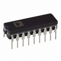
AMP01FX Analog Devices Inc, AMP01FX Datasheet - Page 14

AMP01FX
Manufacturer Part Number
AMP01FX
Description
IC AMP INST PREC LN 120MA 18CDIP
Manufacturer
Analog Devices Inc
Type
Instrumentation Ampr
Specifications of AMP01FX
Rohs Status
RoHS non-compliant
Amplifier Type
Instrumentation
Number Of Circuits
1
Slew Rate
4.5 V/µs
-3db Bandwidth
570kHz
Current - Input Bias
2nA
Voltage - Input Offset
40µV
Current - Supply
3mA
Current - Output / Channel
120mA
Voltage - Supply, Single/dual (±)
±4.5 V ~ 18 V
Operating Temperature
-25°C ~ 85°C
Mounting Type
Through Hole
Package / Case
18-CDIP (0.300", 7.62mm)
Number Of Channels
1
Number Of Elements
1
Power Supply Requirement
Dual
Common Mode Rejection Ratio
75dB
Voltage Gain Db
80dB
Input Resistance
20000@±15VMohm
Input Offset Voltage
0.1@±15VmV
Input Bias Current
6000@±15VnA
Single Supply Voltage (typ)
Not RequiredV
Dual Supply Voltage (typ)
±5/±9/±12/±15V
Rail/rail I/o Type
No
Single Supply Voltage (min)
Not RequiredV
Single Supply Voltage (max)
Not RequiredV
Dual Supply Voltage (min)
±4.5V
Dual Supply Voltage (max)
±18V
Operating Temp Range
-25C to 85C
Operating Temperature Classification
Commercial
Mounting
Through Hole
Pin Count
18
Package Type
CDIP
Application
Used in high-precision data acquisition and instrumentation applications
Bandwidth
570 kHz
Current, Input Bias
2 nA
Current, Input Offset
0.5 nA
Current, Supply
3 mA
Noise, Voltage (rti)
0.12 μV p-p
Resistance, Input
50 Kilohms
Temperature, Operating, Maximum
85 °C
Temperature, Operating, Minimum
-25 °C
Temperature, Operating, Range
-25 to +85 °C
Voltage, Input
-10.5 to +15 V
Voltage, Input Offset
40 μV
Voltage, Noise
540 nV/sqrt Hz
Voltage, Offset, Input
40 μV (Typ.) @ 25 °C
Voltage, Output Swing
±13.8 V
Voltage, Supply
±4.5 to ±18 V
Low Offset Voltage
50 mV Max
Very Low Offset Voltage Drift
0.3 mV⁄8C Max
Excellent Output Drive
610 V at 650 mA
Capacitive Load Stability
to 1 mF
Gain Range
0.1 to 10,000
Excellent Linearity
16-Bit at G == 1000
No. Of Amplifiers
1
Amplifier Output
Differential
Cmrr
125dB
Supply Voltage Range
± 4.5V To ± 18V
Supply Current
3.4mA
Rohs Compliant
No
Output Type
-
Gain Bandwidth Product
-
Lead Free Status / Rohs Status
Not Compliant
Available stocks
Company
Part Number
Manufacturer
Quantity
Price
Part Number:
AMP01FX
Manufacturer:
ADI/亚德诺
Quantity:
20 000
AMP01
If heavy output currents are expected and the load is situated
some distance from the amplifier, voltage drops due to track or
wire resistance will cause errors. Voltage drops are particularly
troublesome when driving 50
the sense and reference terminals can be used to “remote sense”
the load as shown in Figure 33. This method of connection puts
the I R drops inside the feedback loop and virtually eliminates
the error. An unbalance in the lead resistances from the sense
and reference pins does not degrade CMR, but will change the
output offset voltage. For example, a large unbalance of 3
change the output offset by only 1 mV.
DRIVING 50
Output currents of 50 mA are guaranteed into loads of up to
50
and free from oscillation even with a high load capacitance. The
and 26 mA into 500 . In addition, the output is stable
+IN
–IN
LOADS
POWER BANDWIDTH, G = 100, 130kHz
POWER BANDWIDTH, G = 10, 200kHz
T.H.D.~0.04% @ 1kHz, 2Vrms
RESISTERS R1 AND R2 REDUCE IC DISSIPATION
VOLTAGE GAIN, G =
R
G
18
1
2
3
+IN
–IN
14
loads. Under these conditions,
AMP01
R
S
(
20
15
R
G
R
R
V+
V–
S
G
12
11
)
18
1
2
3
13
10
Figure 33. Remote Load Sensing
Figure 34. Driving 50
7
8
14
SENSE
REFERENCE
5k
R
AMP01
S
*
9
OUTPUT
GROUND
IN4148 DIODES ARE OPTIONAL. DIODES LIMIT THE OUTPUT
VOLTAGE EXCURSION IF SENSE AND/OR REFERENCE LINES
BECOME DISCONNECTED FROM THE LOAD.
15
will
–14–
12
11
130
*
*
1W
130
R1
1W
R2
combination of these unique features in an instrumentation
amplifier allows low-level transducer signals to be conditioned
and directly transmitted through long cables in voltage or cur-
rent form. Increased output current brings increased internal
dissipation, especially with 50
power-supply connections are split into two pairs; pins 10 and
13 connect to the output stage only and pins 11 and 12 provide
power to the input and following stages. Dual supply pins allow
dropper resistors to be connected in series with the output stage
so excess power is dissipated outside the package. Additional
decoupling is necessary between pins 10 and 13 to ground to
maintain stability when dropper resistors are used. Figure 34
shows a complete circuit for driving 50
13
10
Loads
REFERENCE
7
8
SENSE
0.047 F
C1
0.047 F
C2
9
TWISTED
PAIRS
0.047 F
0.047 F
loads. For this reason, the
V
50
LOAD
+15V
–15V
OUT
3V MAX
loads.
REMOTE
LOAD
REV. D


