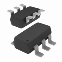
NCV2002SN1T1G ON Semiconductor, NCV2002SN1T1G Datasheet - Page 10

NCV2002SN1T1G
Manufacturer Part Number
NCV2002SN1T1G
Description
IC OPAMP R-R 0.9V 1A 6-TSOP
Manufacturer
ON Semiconductor
Datasheet
1.NCS2002SN1T1G.pdf
(16 pages)
Specifications of NCV2002SN1T1G
Amplifier Type
General Purpose
Number Of Circuits
1
Output Type
Rail-to-Rail
Slew Rate
1.3 V/µs
Gain Bandwidth Product
900kHz
Current - Input Bias
10pA
Voltage - Input Offset
500µV
Current - Supply
820µA
Current - Output / Channel
128mA
Voltage - Supply, Single/dual (±)
0.9 V ~ 7 V, ±0.45 V ~ 3.5 V
Operating Temperature
-40°C ~ 125°C
Mounting Type
Surface Mount
Package / Case
SC-74-6
Number Of Channels
1
Voltage Gain Db
92.04 dB
Common Mode Rejection Ratio (min)
60 dB
Input Voltage Range (max)
Positive Rail
Input Voltage Range (min)
Negative Rail
Input Offset Voltage
6 mV
Operating Supply Voltage
7 V
Supply Current
2 uA
Maximum Power Dissipation
340 mW
Maximum Operating Temperature
+ 125 C
Mounting Style
SMD/SMT
Maximum Dual Supply Voltage
+/- 3.5 V
Minimum Operating Temperature
- 40 C
Lead Free Status / RoHS Status
Lead free / RoHS Compliant
-3db Bandwidth
-
Lead Free Status / Rohs Status
Details
Other names
NCV2002SN1T1G
NCV2002SN1T1GOSTR
NCV2002SN1T1GOSTR
GENERAL INFORMATION
rail−to−rail output amplifier that features guaranteed sub
one volt operation. This unique feature set is achieved with
the use of a modified analog CMOS process that allows the
implementation of depletion MOSFET devices. The
amplifier has a 1.0 MHz gain bandwidth product, 1.2 V/ms
slew rate and is operational over a power supply range less
than 0.9 V to as high as 7.0 V.
Inputs
unconventional when compared to most low voltage
operational amplifiers. It consists of an N−channel depletion
mode differential transistor pair that drives a folded cascade
stage and current mirror. This configuration extends the
input common mode voltage range to encompass the V
and V
combined total of less than 0.9 volts. Figures 27, 28 and 29
show the input common mode voltage range versus power
supply voltage.
minimize offset voltage. The N−channel depletion mode
MOSFET input stage exhibits an extremely low input bias
current of less than 10 pA. The input bias current versus
temperature is shown in Figure 4. Either one or both inputs
can be biased as low as V
7.0 V without causing damage to the device. If the input
common mode voltage range is exceeded, the output will not
display a phase reversal. If the maximum input positive or
negative voltage ratings are to be exceeded, a series resistor
must be used to limit the input current to less than 2.0 mA.
The NCS2002 is an industry first rail−to−rail input,
The input topology chosen for this device series is
The differential input stage is laser trimmed in order to
CC
power supply rails, even when powered from a
APPLICATION INFORMATION AND OPERATING DESCRIPTION
EE
minus 300 mV to as high as
8.0
6.0
4.0
2.0
Figure 32. Propagation Delay versus Supply Voltage
16
14
12
10
0
0
±0.5
±1.0
V
http://onsemi.com
S
, SUPPLY VOLTAGE (V)
EE
±1.5
10
t
t
on
off
±2.0
the use of extremely high value source and feedback resistor
without reducing the amplifier’s gain accuracy. These high
value resistors, in conjunction with the device input and
printed circuit board parasitic capacitances C
additional pole to the single pole amplifier in Figure 33. If
low enough in frequency, this additional pole can reduce the
phase margin and significantly increase the output settling
time. The effects of C
into the feedback loop. This is accomplished with the
addition of capacitor C
be calculated by:
The ultra low input bias current of the NCS2002 allows
Figure 33. Input Capacitance Pole Cancellation
Input
±2.5
C
in
= Input and printed circuit board capacitance
R
T
A
L
±3.0
= 25°C
= 10 k
R
in
C fb +
C
±3.5
in
in
fb
, can be canceled by placing a zero
. An approximate value for C
R in
C
fb
R fb
+
−
R
C in
fb
in
Output
, will add an
fb
can


