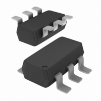
NCV2002SN1T1G ON Semiconductor, NCV2002SN1T1G Datasheet - Page 3

NCV2002SN1T1G
Manufacturer Part Number
NCV2002SN1T1G
Description
IC OPAMP R-R 0.9V 1A 6-TSOP
Manufacturer
ON Semiconductor
Datasheet
1.NCS2002SN1T1G.pdf
(16 pages)
Specifications of NCV2002SN1T1G
Amplifier Type
General Purpose
Number Of Circuits
1
Output Type
Rail-to-Rail
Slew Rate
1.3 V/µs
Gain Bandwidth Product
900kHz
Current - Input Bias
10pA
Voltage - Input Offset
500µV
Current - Supply
820µA
Current - Output / Channel
128mA
Voltage - Supply, Single/dual (±)
0.9 V ~ 7 V, ±0.45 V ~ 3.5 V
Operating Temperature
-40°C ~ 125°C
Mounting Type
Surface Mount
Package / Case
SC-74-6
Number Of Channels
1
Voltage Gain Db
92.04 dB
Common Mode Rejection Ratio (min)
60 dB
Input Voltage Range (max)
Positive Rail
Input Voltage Range (min)
Negative Rail
Input Offset Voltage
6 mV
Operating Supply Voltage
7 V
Supply Current
2 uA
Maximum Power Dissipation
340 mW
Maximum Operating Temperature
+ 125 C
Mounting Style
SMD/SMT
Maximum Dual Supply Voltage
+/- 3.5 V
Minimum Operating Temperature
- 40 C
Lead Free Status / RoHS Status
Lead free / RoHS Compliant
-3db Bandwidth
-
Lead Free Status / Rohs Status
Details
Other names
NCV2002SN1T1G
NCV2002SN1T1GOSTR
NCV2002SN1T1GOSTR
DC ELECTRICAL CHARACTERISTICS
Output Voltage Swing, Low State Output (V
T
V
V
V
Common Mode Rejection Ratio (V
Power Supply Rejection Ratio (V
Output Short Circuit Current
Power Supply Current (Per Amplifier, V
T
Enable Input Threshold Voltage (V
Enable Input Current (V
A
A
CC
CC
CC
= −40 to +125°C
= −40 to +125°C
R
R
R
R
R
R
V
V
V
V
V
V
Operating
Disabled
Enable = 5.0 V
Enable = GND
= 0.45 V, V
= 1.5 V, V
= 2.5 V, V
CC
CC
CC
CC
CC
CC
L
L
L
L
L
L
= 10 k
= 2.0 k
= 10 k
= 2.0 k
= 10 k
= 2.0 k
Source Current High Output State
Sink Current Low Output State
Source Current High Output State
Sink Current Low Output State
Source Current High Output State
Sink Current Low Output State
Venable = V
Venable = V
Venable = V
Venable = V
Venable = V
Venable = V
= 0.45 V, V
= 1.5 V, V
= 2.5 V, V
= 0.5 V to V
= 1.5 V to V
= 2.5 V to V
EE
EE
EE
= −1.5 V
= −2.5 V
EE
EE
= −0.45 V
CC
EE
CC
EE
CC
EE
EE
EE
EE
EE
= −1.5 V, V
= −2.5 V, V
= −0.45 V, V
= −0.5 V
= −1.5 V
= −2.5 V
CC
= 5.0 V, V
Rating
ID
ID
CC
in
CC
ID
= $0.5 V
= $0.5 V
= 0.5 V to 2.5 V, V
= 0 to 5.0 V)
EE
= $0.4 V
= 2.5 V, V
O
= 0)
= 0 V)
ID
(V
= − 0.5 V)
EE
CC
= −2.5 V)
= 2.5 V, V
EE
http://onsemi.com
= −2.5 V)
EE
= −2.5 V, V
3
Symbol
CMRR
V
CM
PSRR
I
Enable
V
th(EN)
I
SC
I
OL
D
= V
O
= 0 V, R
1.7 V + V
Min
0.5
60
60
25
65
L
−
−
−
−
−
−
−
−
−
−
−
−
−
−
−
−
−
−
to GND, T
EE
2.7 V + V
A
−0.446
−0.432
−1.497
−1.484
−2.496
−2.481
−128
−3.0
= 25°C, unless otherwise noted)
Typ
−58
480
720
820
1.0
1.5
2.2
2.5
1.9
1.1
1.1
82
85
32
86
EE
2.8 V + V
−0.40
−0.35
−1.45
−1.40
−2.45
−2.40
−100
1000
Max
−2.0
−45
600
900
3.0
5.0
5.0
2.0
2.0
−
−
−
−
−
−
EE
Unit
mA
mA
dB
dB
mA
V
V


