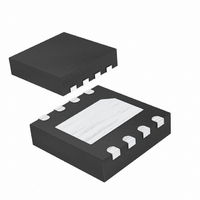
MAX4070ATA+T Maxim Integrated Products, MAX4070ATA+T Datasheet - Page 2

MAX4070ATA+T
Manufacturer Part Number
MAX4070ATA+T
Description
IC AMP CURRENT SENSE 8-TDFN
Manufacturer
Maxim Integrated Products
Datasheet
1.MAX4071ATAT.pdf
(18 pages)
Specifications of MAX4070ATA+T
Amplifier Type
Current Sense
Number Of Circuits
1
-3db Bandwidth
100kHz
Current - Input Bias
2.4µA
Voltage - Input Offset
80µV
Current - Supply
100µA
Voltage - Supply, Single/dual (±)
3.6 V ~ 24 V
Operating Temperature
-40°C ~ 125°C
Mounting Type
Surface Mount
Package / Case
8-TDFN Exposed Pad
Lead Free Status / RoHS Status
Lead free / RoHS Compliant
Output Type
-
Current - Output / Channel
-
Slew Rate
-
Gain Bandwidth Product
-
ABSOLUTE MAXIMUM RATINGS
V
OUT to GND ....................-0.3V to Lesser of (V
Differential Input Voltage (V
GSEL, SHDN, REFOUT, REFIN
OUT Short-Circuit Duration to GND
REFOUT Short Circuit to V
Current into Any Pin ..........................................................±20mA
Bidirectional, High-Side, Current-Sense
Amplifiers with Reference
Stresses beyond those listed under “Absolute Maximum Ratings” may cause permanent damage to the device. These are stress ratings only, and functional
operation of the device at these or any other conditions beyond those indicated in the operational sections of the specifications is not implied. Exposure to
absolute maximum rating conditions for extended periods may affect device reliability.
ELECTRICAL CHARACTERISTICS
(V
T
2
Operating Voltage Range
(Note 3)
Input-Referred Offset Voltage
(Note 5)
Common-Mode Input Range
Common-Mode Rejection Ratio
Supply Current
Shutdown Supply Current
Leakage Current
Input Bias Current
Recommended Full-Scale Sense
Voltage (Note 6)
CC
A
RS
and ADJ to GND.....................................-0.3V to (V
or to Lesser of (V
= T
, RS+, RS- to GND ...........................................-0.3V to +26V
_______________________________________________________________________________________
+ = V
MIN
RS
to T
PARAMETER
- = V
MAX
CC
, unless otherwise noted. Typical values are at T
CC
= 2.7V to 24V, V
or 15V) ...................................Continuous
CC
RS
or GND........................Continuous
+ - V
RS
SENSE
- ) ..............................±0.3V
SYMBOL
I
I
CC SHDN
RS+,
V
CMRR
CMVR
SENSE
V
V
I
CC
CC
OS
= V
I
RS-
CC
RS
+ 0.3V) or 15V
+ - V
MAX4069/MAX4071/MAX4072 (Note 4)
MAX4070
V
V
Guaranteed by CMRR test
1.35V ≤ V
V
T
V
SHDN = GND, T
V
SHDN = GND
V
V
Gain = 50V/V
Gain = 100V/V
A
CC
RS-
CC
CC
CC
RS+
CC
CC
= T
RS
= V
= V
= V
= V
= V
= 12V
+ 0.3V)
= V
- = 0V, I
MIN
RS+
RS+
RS+
RS+
RS+
RS-
RS+
to T
=
= V
= V
= V
= V
= 24V, V
= V
REFOUT
MAX
CONDITIONS
A
RS-
RS-
RS-
RS-
A
= +25°C and at V
RS-
= +25°C
T
T
T
Continuous Power Dissipation (T
Operating Temperature Range .........................-40°C to +125°C
Junction Temperature ......................................................+150°C
Storage Temperature Range .............................-65°C to +150°C
Lead Temperature (soldering, 10s) .................................+300°C
= 24V, R
= 5.5V,
= 24V,
= 24V
A
A
A
≤ 24V, V
CC
8-Pin µMAX (derate 4.5 mW/°C above +70°C) ............362mW
8-Pin Thin QFN (derate 24.4mW/°C above +70°C) ...1951mW
10-Pin µMAX (derate 5.6 mW/°C above +70°C) .......444.4mW
= +25°C
= -40°C to +85°C
= T
= 0, V
= 0V
MIN
L
SHDN
CC
to T
= open,
= 12V
MAX
= V
CC
CC
= V
, V
RS
GSEL
+ = 12V.) (Notes 1, 2)
MIN
1.35
100
= GND, V
2.7
3.6
0
A
= +70°C)
TYP
0.08
120
100
0.1
2.4
REFIN
10
75
50
9
= 2.5V (MAX4072),
MAX
0.25
250
0.8
0.5
24
24
24
30
1
5
UNITS
mV
mV
dB
µA
µA
µA
µA
V
V


