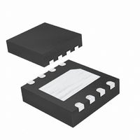
MAX4070ATA+T Maxim Integrated Products, MAX4070ATA+T Datasheet - Page 5

MAX4070ATA+T
Manufacturer Part Number
MAX4070ATA+T
Description
IC AMP CURRENT SENSE 8-TDFN
Manufacturer
Maxim Integrated Products
Datasheet
1.MAX4071ATAT.pdf
(18 pages)
Specifications of MAX4070ATA+T
Amplifier Type
Current Sense
Number Of Circuits
1
-3db Bandwidth
100kHz
Current - Input Bias
2.4µA
Voltage - Input Offset
80µV
Current - Supply
100µA
Voltage - Supply, Single/dual (±)
3.6 V ~ 24 V
Operating Temperature
-40°C ~ 125°C
Mounting Type
Surface Mount
Package / Case
8-TDFN Exposed Pad
Lead Free Status / RoHS Status
Lead free / RoHS Compliant
Output Type
-
Current - Output / Channel
-
Slew Rate
-
Gain Bandwidth Product
-
ELECTRICAL CHARACTERISTICS (continued)
(V
T
Note 1: All devices are 100% tested at T
Note 2: R1 = 215kΩ, R2 = 210kΩ for the MAX4069 only (see Functional Diagram ). This sets REFOUT to 2.49V nominal.
Note 3: Guaranteed by the PSRR test.
Note 4: The REFOUT voltage for the MAX4069 should be set such that it does not exceed V
Note 5: Input-Referred Offset Voltage is defined as the voltage difference between OUT and REFOUT, divided by the selected gain
Note 6: The negative full-scale sense voltage is limited by the voltage range of OUT from V
Note 7: Total OUT Voltage Error is the sum of offset voltage and gain errors. The output voltage is measured relative to the reference
REFOUT (MAX4069/MAX4070/MAX4071)
Reference Output Voltage
Reference Output Voltage
Temperature Coefficient
Load Regulation
Line Regulation
REF Capacitive-Load Stability
Reference Adjust Voltage
Threshold
Reference Output Voltage Range
Reference Adjust Input Current
REFIN (MAX4072 only)
Input-Voltage Range
Input Current
A
RS
= T
+ = V
MIN
voltage for the MAX4072 should also be less than V
of either 50 or 100, when V
(REFOUT or REFIN).
RS
to T
PARAMETER
- = V
MAX
CC
, unless otherwise noted. Typical values are at T
= 2.7V to 24V, V
_______________________________________________________________________________________
Bidirectional, High-Side, Current-Sense
SENSE
SENSE
ΔV
SYMBOL
TCV
ΔV
/ΔI
ΔV
V
V
REFOUT
I
A
ADJ
REF
ADJ
REF/
REF
= V
CC
REF
= +25°C. Limits over temperature are guaranteed by design.
= V
RS+
RS
+ - V
MAX4069,
V
(Note 2)
MAX4070,
V
MAX4071,
V
V
I
I
2.7V ≤ V
MAX4069, V
MAX4069, range adjustable with R1 and R2,
V
MAX4069, V
V
REFIN = 2.5V, V
- V
REFOUT
REFOUT
CC
CC
CC
CC
CC
CC
RS-
RS
= 12V
= 12V
= 12V
= 12V
= 12V
= 12V
- = 0V, I
= 0V.
CC
= 0 to 500µA
= 0 to -100µA
CC
Amplifiers with Reference
≤ 24V
CC
CC
- 1.1V.
REFOUT
A
CONDITIONS
= 12V
= 12V, V
CC
= +25°C and at V
T
T
T
T
T
T
-40°C ≤ T
T
A
A
A
A
A
A
A
= 12V
= +25°C
= +25°C
= +25°C
= T
= T
= T
= T
= 0, V
MIN
MIN
MIN
MIN
ADJ
A
SHDN
to T
to T
to T
to T
= 1.23V
≤ +85°C
MAX
MAX
MAX
MAX
= V
CC
CC
= V
, V
REFOUT
RS
CC
GSEL
+ = 12V.) (Notes 1, 2)
- 1.1V. Similarly, the maximum REFIN
2.44
2.39
2.45
2.40
1.47
1.44
= GND, V
MIN
-60
to GND.
1
V
1.230
ADJ
TYP
2.49
500
100
REFIN
2.5
1.5
+4
15
20
20
2
4
to
= 2.5V (MAX4072),
MAX
2.54
2.59
2.55
2.60
1.53
1.56
+20
4
ppm/°C
mV/mA
UNITS
µV/V
pF
nA
µA
V
V
V
V
5


