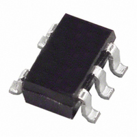
AD8517ART-REEL Analog Devices Inc, AD8517ART-REEL Datasheet

AD8517ART-REEL
Specifications of AD8517ART-REEL
Available stocks
Related parts for AD8517ART-REEL
AD8517ART-REEL Summary of contents
Page 1
GENERAL DESCRIPTION The AD8517 brings precision and bandwidth to the SOT-23-5 package even at single supply voltages as low as 1.8 V. The small package makes it possible to place the AD8517 next to sensors, reducing external noise pickup. ...
Page 2
... AD8517/AD8527–SPECIFICATIONS ELECTRICAL CHARACTERISTICS Parameter INPUT CHARACTERISTICS Offset Voltage AD8517ART (SOT-23-5) AD8527 Input Bias Current Input Offset Current Input Voltage Range Common-Mode Rejection Ratio Large Signal Voltage Gain Offset Voltage Drift Bias Current Drift OUTPUT CHARACTERISTICS Output Voltage Swing High Output Voltage Swing Low ...
Page 3
... ELECTRICAL CHARACTERISTICS Parameter INPUT CHARACTERISTICS Offset Voltage AD8517ART (SOT-23-5) AD8527 Input Bias Current Input Offset Current Input Voltage Range Common-Mode Rejection Ratio Large Signal Voltage Gain OUTPUT CHARACTERISTICS Output Voltage Swing High Output Voltage Swing Low POWER SUPPLY Supply Current/Amplifier DYNAMIC PERFORMANCE ...
Page 4
... AD8517/AD8527–SPECIFICATIONS ELECTRICAL CHARACTERISTICS Parameter INPUT CHARACTERISTICS Offset Voltage AD8517ART (SOT-23-5) AD8527 Input Bias Current Input Offset Current Input Voltage Range Common-Mode Rejection Ratio Large Signal Voltage Gain OUTPUT CHARACTERISTICS Output Voltage Swing High Output Voltage Swing Low POWER SUPPLY Power Supply Rejection Ratio ...
Page 5
... AD8517, AD8527 . . . . . . . . . . . . . . . . . . –40°C to +125°C Junction Temperature Range R, RM and RT Packages . . . . . . . . . . . . . –65°C to +150°C Lead Temperature Range (Soldering, 60 sec 300°C Model AD8517ART-REEL AD8527AR AD8527ARM-REEL CAUTION ESD (electrostatic discharge) sensitive device. Electrostatic charges as high as 4000 V readily accumulate on the human body and test equipment and can discharge without detection. ...
Page 6
AD8517/AD8527 –Typical Characteristics 1,200 1,100 1,000 900 800 700 600 TEMPERATURE – C 600 400 200 0 200 400 600 3 2 ...
Page 7
PSRR 100 120 10 100 1k 10k 100k FREQUENCY – 2. 10k L T ...
Page 8
AD8517/AD8527 TIME – 1s/Div TIME – 200 s/Div THEORY OF OPERATION The AD85x7 is a rail-to-rail operational ...
Page 9
ESD ESD R9 I2 Table I. Typical Battery Life Voltage Range Nominal Battery Voltage (V) Lead-Acid 2 Lithium 2.6-3.6 NiMH 1.2 NiCd 1.2 Carbon-Zinc 1.5 ...
Page 10
AD8517/AD8527 DRIVING CAPACITIVE LOAD Gain vs. Capacitive Load Most amplifiers have difficulty driving capacitance due to degradation of phase caused by additional phase lag from the capacitive load. Higher capacitance at the output can increase the amount of over- shoot ...
Page 11
Table III. Snubber Network Values for Large Capacitive Loads C Rx LOAD 300 Ω 680 pF 100 Ω 400 Ω TOTAL HARMONIC DISTORTION + NOISE The AD85x7 family offers a low total harmonic distortion, which makes ...
Page 12
AD8517/AD8527 SPICE Model The SPICE model for the AD8517 amplifier is available and can be downloaded from the Analog Devices’ web site at http://www.analog.com. The macro-model accurately simulates a number of AD8517 parameters, including offset voltage, input common-mode range, and ...


