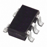
AD8517ART-REEL Analog Devices Inc, AD8517ART-REEL Datasheet - Page 8

AD8517ART-REEL
Manufacturer Part Number
AD8517ART-REEL
Description
IC OPAMP GP R-R 7MHZ SOT23-5
Manufacturer
Analog Devices Inc
Datasheet
1.AD8517ART-R2.pdf
(12 pages)
Specifications of AD8517ART-REEL
Rohs Status
RoHS non-compliant
Amplifier Type
General Purpose
Number Of Circuits
1
Output Type
Rail-to-Rail
Slew Rate
8 V/µs
Gain Bandwidth Product
7MHz
Current - Input Bias
450nA
Voltage - Input Offset
1300µV
Current - Supply
900µA
Current - Output / Channel
10mA
Voltage - Supply, Single/dual (±)
1.8 V ~ 6 V
Operating Temperature
-40°C ~ 125°C
Mounting Type
Surface Mount
Package / Case
SOT-23-5, SC-74A, SOT-25
-3db Bandwidth
-
Available stocks
Company
Part Number
Manufacturer
Quantity
Price
Company:
Part Number:
AD8517ART-REEL7
Manufacturer:
AD
Quantity:
5 510
Company:
Part Number:
AD8517ART-REEL7
Manufacturer:
AVX
Quantity:
5 510
Part Number:
AD8517ART-REEL7
Manufacturer:
ADI/亚德诺
Quantity:
20 000
AD8517/AD8527
THEORY OF OPERATION
The AD85x7 is a rail-to-rail operational amplifier that can operate at
supply voltages as low as 1.8 V. This family is fabricated using Analog
Devices’ high-speed complementary bipolar process, also called
XFCB. The process trench isolates each transistor to minimize
parasitic capacitance thereby allowing high-speed performance.
Figure 19 shows a simplified schematic of the AD85x7 family.
The input stage consists of two parallel complementary differen-
tial pair: one NPN pair (Q1 and Q2) and one PNP pair (Q3 and
Q4). The voltage drops across R7. R8, R9, and R10 are kept low
for rail-to-rail operation. The major gain stage of the op amp is a
double-folded cascode consisting of transistors Q5, Q6, Q8, and
Q9. The output stage, which also operates rail-to-rail, is driven by
Q14. The transistors Q13 and Q10 act as level-shifters to give
more headroom during 1.8 V operation.
As the voltage at the base of Q13 increases, Q18 starts to sink
current. When the voltage at the base of Q13 decreases, I8 flows
through D16 and Q15 increasing the VBE of Q17, then Q20
sources current.
The output stage also furnishes gain, which depends on the load
resistance, since the output transistors are in common emitter
0
0
0
0
0
0
0
0
TIME – 200 s/Div
TIME – 1s/Div
V
A
V
T
A
S
IN
V
=
= 25 C
= + 1
= SINEWAVE
2.5V
V
A
T
S
A
V
=
= 120k
= 25 C
2.5V
configuration. The output swing when sinking or sourcing 250 µA
is 35 mV from each rail.
The input bias current characteristics depend on the common-
mode voltage, see Figure 4. As the input voltage reaches about
1 V below V
The 1 kΩ input resistor R1 and R2, together with the diodes D7
and D8, protect the input pairs against avalanche damage.
The AD85x7 family exhibits no phase reversal as the input
signal exceeds the supply by more than 0.6 V. Excessive current
can flow through the input pins via the ESD diodes D1–D2 or
D3–D4, in the event their ~0.6 V thresholds are exceeded. Such
fault currents must be limited to 5 mA or less by the use of
external series resistance(s).
LOW VOLTAGE OPERATION
Battery Voltage Discharge
The AD8517 operates at supply voltages as low as 1.8 V. This
amplifier is ideal for battery-powered applications since it can
operate at the end of discharge voltage of most popular batteries.
Table I lists the Nominal and End of Discharge Voltages of several
typical batteries.
V
A
T
C
R
CC
A
S
L
V
L
= 25 C
=
= 100pF
= 10k
, the PNP pair (Q3 and Q4) turns off.
= 1
2.5V
TIME – 200ns/Div
TIME – 500ns/Div
V
A
R
T
A
S
V
L
=
= 10k
= 25 C
= 1
2.5V


