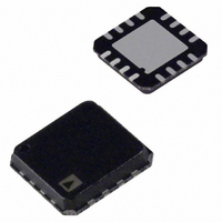
AD8555ACP-REEL7 Analog Devices Inc, AD8555ACP-REEL7 Datasheet - Page 17

AD8555ACP-REEL7
Manufacturer Part Number
AD8555ACP-REEL7
Description
IC AMP CHOPPER 2MHZ 10MA 16LFCSP
Manufacturer
Analog Devices Inc
Series
DigiTrim®r
Datasheet
1.AD8555ARZ.pdf
(28 pages)
Specifications of AD8555ACP-REEL7
Rohs Status
RoHS non-compliant
Amplifier Type
Chopper (Zero-Drift)
Number Of Circuits
1
Slew Rate
1.2 V/µs
Gain Bandwidth Product
2MHz
Current - Input Bias
16nA
Voltage - Input Offset
2µV
Current - Supply
2mA
Current - Output / Channel
10mA
Voltage - Supply, Single/dual (±)
2.7 V ~ 5.5 V
Operating Temperature
-40°C ~ 125°C
Mounting Type
Surface Mount
Package / Case
16-LFCSP
Output Type
-
-3db Bandwidth
-
THEORY OF OPERATION
A1, A2, R1, R2, R3, P1, and P2 form the first gain stage of the
differential amplifier. A1 and A2 are auto-zeroed op amps that
minimize input offset errors. P1 and P2 are digital potentiome-
ters, guaranteed to be monotonic. Programming P1 and P2
allows the first stage gain to be varied from 4.0 to 6.4 with 7-bit
resolution (see Table 6 and Equation 3), giving a fine gain
adjustment resolution of 0.37%. R1, R2, R3, P1, and P2 each
have a similar temperature coefficient, so the first stage gain
temperature coefficient is lower than 100 ppm/°C.
A3, R4, R5, R6, R7, P3, and P4 form the second gain stage of the
differential amplifier. A3 is also an auto-zeroed op amp that
minimize input offset errors. P3 and P4 are digital potentiome-
ters, allowing the second stage gain to be varied from 17.5 to
200 in eight steps (see Table 7); they allow the gain to be varied
over a wide range. R4, R5, R6, R7, P3, and P4 each have a simi-
lar temperature coefficient, so the second stage gain tempera-
ture coefficient is lower than 100 ppm/°C.
RF together with an external capacitor connected between
FILT/DIGOUT and VSS or VDD form a low-pass filter. The
filtered signal is buffered by A4 to give a low impedance output
at VOUT. RF is nominally 16 kΩ, allowing a 1 kHz low-pass
filter to be implemented by connecting a 10 nF external
capacitor between FILT/DIGOUT and VSS or between
FILT/DIGOUT and VDD. If low-pass filtering is not needed,
then the FILT/DIGOUT pin must be left floating.
A5 implements a voltage buffer, which provides the positive
supply to the amplifier output buffer A4. Its function is to limit
VOUT to a maximum value, useful for driving analog-to-digital
converters (ADC) operating on supply voltages lower than
VNEG
VPOS
VDD
A1
VDD
A2
VSS
VSS
Figure 49. AD8555 Functional Schematic
R1
R3
R2
VDD
DAC
VSS
P1
P2
R4
R5
Rev. A | Page 17 of 28
P4
P3
VDD
A3
VSS
R6
R7
VCLAMP
VDD. The input to A5, VCLAMP, has a very high input resis-
tance. It should be connected to a known voltage and not left
floating. However, the high input impedance allows the clamp
voltage to be set using a high impedance source, e.g., a potential
divider. If the maximum value of VOUT does not need to be
limited, VCLAMP should be connected to VDD.
A4 implements a rail-to-rail input and output unity-gain vol-
tage buffer. The output stage of A4 is supplied from a buffered
version of VCLAMP instead of VDD, allowing the positive
swing to be limited. The maximum output current is limited
between 5 mA to 10 mA.
An 8-bit digital-to-analog converter (DAC) is used to generate a
variable offset for the amplifier output. This DAC is guaranteed
to be monotonic. To preserve the ratiometric nature of the input
signal, the DAC references are driven from VSS and VDD, and
the DAC output can swing from VSS (Code 0) to VDD (Code
255). The 8-bit resolution is equivalent to 0.39% of the differ-
ence between VDD and VSS, e.g., 19.5 mV with a 5 V supply.
The DAC output voltage (VDAC) is given approximately by
The temperature coefficient of VDAC is lower than
200 ppm/°C.
The amplifier output voltage (VOUT) is given by
where GAIN is the product of the first and second stage gains.
RF
DIGOUT
FILT/
VDAC
VOUT
VDD
A5
VSS
≈
=
VDD
A4
⎛
⎜
⎝
GAIN
VSS
Code
256
(
+
VPOS
VOUT
0
5 .
⎞
⎟
⎠
(
−
VDD
VNEG
−
VSS
)
+
VDAC
)
+
VSS
AD8555
(1)
(2)


