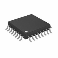
ADM1069ASTZ Analog Devices Inc, ADM1069ASTZ Datasheet - Page 21

ADM1069ASTZ
Manufacturer Part Number
ADM1069ASTZ
Description
IC SUPERVISOR/SEQUENCER 32-LQFP
Manufacturer
Analog Devices Inc
Type
Sequencerr
Datasheet
1.EVAL-ADM1069LQEBZ.pdf
(32 pages)
Specifications of ADM1069ASTZ
Number Of Voltages Monitored
8
Output
Programmable
Voltage - Threshold
8 Selectable Threshold Combinations
Operating Temperature
-40°C ~ 85°C
Mounting Type
Surface Mount
Package / Case
32-LQFP
For Use With
EVAL-ADM1069LQEBZ - BOARD EVALUATION FOR ADM1069LQ
Lead Free Status / RoHS Status
Lead free / RoHS Compliant
Reset
-
Reset Timeout
-
Available stocks
Company
Part Number
Manufacturer
Quantity
Price
Company:
Part Number:
ADM1069ASTZ
Manufacturer:
AKM
Quantity:
940
Company:
Part Number:
ADM1069ASTZ
Manufacturer:
AD
Quantity:
885
Company:
Part Number:
ADM1069ASTZ
Manufacturer:
Analog Devices Inc
Quantity:
10 000
Part Number:
ADM1069ASTZ
Manufacturer:
ADI/亚德诺
Quantity:
20 000
Company:
Part Number:
ADM1069ASTZ-REEL
Manufacturer:
Analog Devices Inc
Quantity:
10 000
Part Number:
ADM1069ASTZ-REEL
Manufacturer:
ADI/亚德诺
Quantity:
20 000
Company:
Part Number:
ADM1069ASTZ-REEL7
Manufacturer:
Analog Devices Inc
Quantity:
10 000
SUPPLY MARGINING
OVERVIEW
It is often necessary for the system designer to adjust supplies,
either to optimize their level or force them away from nominal
values to characterize the system performance under these
conditions. This is a function typically performed during an
in-circuit test (ICT), such as when a manufacturer wants to
guarantee that a product under test functions correctly at
nominal supplies minus 10%.
OPEN-LOOP SUPPLY MARGINING
The simplest method of margining a supply is to implement
an open-loop technique (see Figure 32). A popular way to do
this is to switch extra resistors into the feedback node of a power
module, such as a dc-to-dc converter or low dropout regulator
(LDO). The extra resistor alters the voltage at the feedback or
trim node and forces the output voltage to margin up or down
by a certain amount.
The ADM1069 can perform open-loop margining for up to four
supplies. The four on-board voltage DACs (DAC1 to DAC4) can
drive into the feedback pins of the power modules to be margined.
The simplest circuit to implement this function is an attenuation
resistor that connects the DACx pin to the feedback node of a
dc-to-dc converter. When the DACx output voltage is set equal
to the feedback voltage, no current flows into the attenuation
resistor, and the dc-to-dc converter output voltage does not change.
Taking DACx above the feedback voltage forces current into the
feedback node, and the output of the dc-to-dc converter is forced
to fall to compensate for this. The dc-to-dc converter output can be
forced high by setting the DACx output voltage lower than the
feedback node voltage. The series resistor can be split in two, and
the node between them can be decoupled with a capacitor to
ground. This can help to decouple any noise picked up from the
board. Decoupling to a ground local to the dc-to-dc converter
is recommended.
The ADM1069 can be commanded to margin a supply up or
down over the SMBus by updating the values on the relevant
DAC output.
CONVERTER
DC-TO-DC
FEEDBACK
VIN
OUTPUT
GND
Figure 32. Open-Loop Margining System Using the ADM1069
R1
R2
ATTENUATION
RESISTOR, R3
V
Rev. B | Page 21 of 32
OUT
PCB
TRACE NOISE
DECOUPLING
CAPACITOR
DACx
CLOSED-LOOP SUPPLY MARGINING
A more accurate and comprehensive method of margining is to
implement a closed-loop system (see Figure 33). The voltage on
the rail to be margined can be read back to accurately margin the
rail to the target voltage. The ADM1069 incorporates all the circuits
required to do this, with the 12-bit successive approximation ADC
used to read back the level of the supervised voltages, and the
six voltage output DACs, implemented as described in the Open-
Loop Supply Margining section, used to adjust supply levels.
These circuits can be used along with other intelligence, such as
a microcontroller, to implement a closed-loop margining system
that allows any dc-to-dc converter or LDO supply to be set to
any voltage, accurate to within ±0.5% of the target.
To implement closed-loop margining,
1.
2.
3.
4.
5.
6.
7.
Step 1 to Step 3 ensure that when the DACx output buffer is
turned on, it has little effect on the dc-to-dc converter output.
The DAC output buffer is designed to power up without
glitching by first powering up the buffer to follow the pin
voltage. It does not drive out onto the pin at this time. Once the
output buffer is properly enabled, the buffer input is switched
over to the DAC, and the output stage of the buffer is turned on.
Output glitching is negligible.
ADM1069
Disable the four DACx outputs.
Set the DAC output voltage equal to the voltage on the
feedback node.
Enable the DAC.
Read the voltage at the dc-to-dc converter output that
is connected to one of the VPx, VH, or VXx pins.
If necessary, modify the DACx output code up or down
to adjust the dc-to-dc converter output voltage. Otherwise,
stop because the target voltage has been reached.
Set the DAC output voltage to a value that alters the supply
output by the required amount (for example, ±5%).
Repeat Step 4 through Step 6 until the measured supply
reaches the target voltage.
DAC
MICROCONTROLLER
CONTROLLER
(SMBus)
DEVICE
ADM1069


