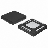
MAX6793TPLD2+ Maxim Integrated Products, MAX6793TPLD2+ Datasheet - Page 2

MAX6793TPLD2+
Manufacturer Part Number
MAX6793TPLD2+
Description
IC REG LIN W/SPR VSR 20-TQFN
Manufacturer
Maxim Integrated Products
Type
Regulator/Supervisorr
Datasheet
1.MAX6796TPLD2T.pdf
(25 pages)
Specifications of MAX6793TPLD2+
Number Of Voltages Monitored
1
Output
Open Drain or Open Collector
Reset
Active Low
Reset Timeout
8.75 ms Minimum
Voltage - Threshold
4.625V
Operating Temperature
-40°C ~ 125°C
Mounting Type
Surface Mount
Package / Case
20-TQFN Exposed Pad
Number Of Outputs
2
Polarity
Positive
Input Voltage Max
72 V
Output Voltage
1.8 V to 11 V, 5 V
Output Type
Adjustable, Fixed
Dropout Voltage (max)
1.8 V at 150 mA
Output Current
150 mA
Line Regulation
1 %
Load Regulation
1.5 %
Maximum Power Dissipation
2.6667 W
Maximum Operating Temperature
+ 125 C
Mounting Style
SMD/SMT
Minimum Operating Temperature
- 40 C
Lead Free Status / RoHS Status
Lead free / RoHS Compliant
ABSOLUTE MAXIMUM RATINGS
(All pins referenced to GND, unless otherwise noted.)
IN to GND ...............................................................-0.3V to +80V
ENABLE, ENABLE1, ENABLE2, PFI,
GATEP to IN ...........................................................-12V to +0.3V
OUT, OUT1, OUT2, PFO, RESET (open-drain versions),
HOLD, RESET (push-pull versions), WDI, WDS0, WDS1,
High-Voltage, Micropower, Single/Dual Linear
Regulators with Supervisory Functions
ELECTRICAL CHARACTERISTICS
(V
(Note 1)
Stresses beyond those listed under “Absolute Maximum Ratings” may cause permanent damage to the device. These are stress ratings only, and functional
operation of the device at these or any other conditions beyond those indicated in the operational sections of the specifications is not implied. Exposure to
absolute maximum rating conditions for extended periods may affect device reliability.
2
Supply Voltage Range
Supply Current
Shutdown Supply Current
GATEP to GND ...........................................-0.3V to (IN + 0.3V)
CSRT, CSWT .......................................................-0.3V to +12V
WD-DIS, SET, SET1......................-0.3V to (OUT/OUT1 + 0.3V)
IN
_______________________________________________________________________________________
= 14V, C
PARAMETER
IN
= 1µF, C
OUT
= 10µF, T
SYMBOL
I
A
SHDN
V
I
IN
= T
IN
J
= -40°C to +125°C, unless otherwise noted. Typical values are at T
Regulators on (I
Regulators on,
OUT/OUT1 =
OUT2 = 5V
Regulators on (I
Regulators on (I
OUT1/OUT2/OUT = 5V, V
Regulators off, V
CONDITIONS
LOAD
LOAD
LOAD
IN
V
(MAX6795/MAX6796)
V
(MAX6795/MAX6796)
V
= 150mA
(MAX6791–MAX6794)
V
I
(MAX6791–MAX6794)
LOAD2
IN
IN
IN
IN
= 14V
OUT, OUT1, OUT2 Short Circuit
Maximum Current (all pins except IN and OUT_)...............50mA
Continuous Power Dissipation (T
Operating Temperature Range (T
Junction Temperature (T
Storage Temperature Range .............................-65°C to +150°C
Lead Temperature (soldering, 10s) .................................+300°C
= 8V, I
= 14V, I
= 8V, I
= 14V, I
to GND....................................................................Continuous
= 0mA), V
= 0mA), V
= 20mA, total)
20-Pin TQFN (derate 33.3mW/°C above +70°C) .....2666.7mW
= 50mA
IN
LOAD
LOAD1
= 42V
LOAD
LOAD1
IN
IN
= 300mA
= 8V
= 42V
= I
= 100mA
=
LOAD2
J
) .................................................150°C
MIN
5
A
A
= +70°C)
) ..................-40°C to +125°C
TYP
130
100
130
100
100
68
74
27
A
MAX
220
160
220
160
170
72
85
95
45
= T
J
= +25°C.)
UNITS
µA
µA
V


