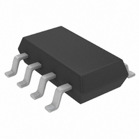
LTC2909CTS8-3.3#TRPBF Linear Technology, LTC2909CTS8-3.3#TRPBF Datasheet - Page 6

LTC2909CTS8-3.3#TRPBF
Manufacturer Part Number
LTC2909CTS8-3.3#TRPBF
Description
IC MONITOR PREC 3.3V TSOT23-8
Manufacturer
Linear Technology
Type
Multi-Voltage Supervisorr
Datasheet
1.LTC2909CDDB-5TRPBF.pdf
(16 pages)
Specifications of LTC2909CTS8-3.3#TRPBF
Number Of Voltages Monitored
3
Output
Open Drain or Open Collector
Reset
Active Low
Reset Timeout
Adjustable/Selectable
Voltage - Threshold
2.921V, Adj, Adj
Operating Temperature
0°C ~ 70°C
Mounting Type
Surface Mount
Package / Case
TSOT-23-8, TSOT-8
Lead Free Status / RoHS Status
Lead free / RoHS Compliant
Available stocks
Company
Part Number
Manufacturer
Quantity
Price
Part Number:
LTC2909CTS8-3.3#TRPBFLTC2909CTS8-3.3#PBF
Manufacturer:
LINEAR/凌特
Quantity:
20 000
PI FU CTIO S
LTC2909
ADJ1 (Pin 1/Pin 8): Adjustable Voltage Input 1. Input to
voltage monitor comparator 1 (0.5V nominal threshold).
The polarity of the input is selected by the state of the
SEL pin (refer to Table 1). Tie to REF if unused (with SEL
= V
ADJ2 (Pin 2/Pin 7): Adjustable Voltage Input 2. Input to
voltage monitor comparator 2 (0.5V nominal threshold).
The polarity of the input is selected by the state of the
SEL pin (refer to Table 1). Tie to GND if unused (with SEL
= GND or Open).
REF (Pin 3/Pin 6): Buffered Reference Output. 1V nominal
reference used for the offset of negative-monitoring appli-
cations. The buffered reference can source and sink 1mA.
The reference can drive a capacitive load of up to 1000pF.
Larger capacitance may degrade transient performance.
This pin does not require a bypass capacitor, nor is one
recommended. Leave open if unused.
GND (Pin 4/Pin 5): Device Ground.
⎯ R ⎯ S ⎯ T (Pin 5/Pin 4): Open-Drain Inverted Reset Logic Output.
Asserts low when any positive polarity input voltage is
below threshold or any negative polarity input voltage is
above threshold or V
for a timeout after all voltage inputs are valid. Requires an
external pull-up resistor and may be pulled above V
6
U
CC
or Open).
U
CC
U
is below UVLO threshold. Held low
(TSOT-23/DFN Package)
CC
.
V
ground with a 0.1μF (or greater) capacitor. Operates as
a direct supply input for voltages up to 6V. Operates as a
shunt regulator for supply voltages greater than 6V and
should have a resistor between this pin and the supply
to limit V
used without a current-limiting resistor, pin voltage must
not exceed 6V. UVLO options allow V
accurate third fi xed 10% UV supply monitor.
TMR (Pin 7/Pin 2): Reset Timeout Control. Attach an
external capacitor (C
of 9ms/nF. A low leakage ceramic capacitor is recom-
mended for timer accuracy. Capacitors larger than 1μF
(9 second timeout) are not recommended. See Applica-
tions Information for further details. Leaving this pin open
generates a minimum timeout of approximately 400μs. A
2.2nF capacitor will generate a 20ms timeout. Tying this
pin to ground will enable the internal 200ms timeout. Ty-
ing this pin to V
part in comparator mode. Signals from the comparator
outputs will then go directly to ⎯ R ⎯ S ⎯ T .
SEL (Pin 8/Pin 1): Input Polarity Select Three-State Input.
Connect to V
to select one of three possible input polarity combinations
(refer to Table 1).
Exposed Pad (Pin 9, DFN Only): The Exposed Pad may be
left unconnected. For better thermal contact, tie to a PCB
trace. This trace must be grounded or unconnected.
CC
(Pin 6/Pin 3): Power Supply. Bypass this pin to
CC
input current to no greater than 10mA. When
CC
, GND or leave unconnected in open state
CC
will disable the reset timer and put the
TMR
) to GND to set a reset timeout
CC
to be used as an
2909fb


