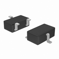
XC61CN2302MR-G Torex Semiconductor Ltd, XC61CN2302MR-G Datasheet - Page 6

XC61CN2302MR-G
Manufacturer Part Number
XC61CN2302MR-G
Description
IC SUPERVISOR 2.3V SOT23-3
Manufacturer
Torex Semiconductor Ltd
Type
Simple Reset/Power-On Resetr
Datasheet
1.XC61CN3002MR-G.pdf
(18 pages)
Specifications of XC61CN2302MR-G
Number Of Voltages Monitored
1
Output
Open Drain or Open Collector
Voltage - Threshold
2.3V
Operating Temperature
-40°C ~ 85°C
Mounting Type
Surface Mount
Package / Case
SOT-23-3, TO-236-3, Micro3™, SSD3, SST3
Lead Free Status / RoHS Status
Lead free / RoHS Compliant
Reset
-
Reset Timeout
-
6/18
■NOTES ON USE
●Oscillation Description
1. Please use this IC within the stated absolute maximum ratings. For temporary, transitional voltage drop or voltage rising
7. Torex places an importance on improving our products and its reliability.
2. When a resistor is connected between the V
3. When a resistor is connected between the V
4. Please use N-ch open drain output configuration, when a resistor R
5. With a resistor R
6. In order to stabilize the IC's operations, please ensure that V
(1) Load current oscillation with the CMOS output configuration
(2) Oscillation as a result of through current
XC61C
When the voltage applied at power supply, release operations commence and the detector's output voltage increases.
Load current (I
power supply and the V
voltage level at the V
commence. Following detect operations, load current flow will cease and since voltage drop at R
voltage level at the V
Oscillation may occur with this " release - detect - release " repetition.
Further, this condition will also appear via means of a similar mechanism during detect operations.
Since the XC61C series are CMOS IC
release and detect operations). Consequently, oscillation is liable to occur as a result of drops in voltage at the through
current's resistor (R
Since hysteresis exists during detect operations, oscillation is unlikely to occur.
However, by any possibility, we would request user fail-safe design and post-aging treatment on system or equipment.
occur as a result of voltage drops at R
N-ch open-drain output configurations, oscillation may occur as a result of through current at the time of voltage release even
if load current (I
In such cases, please ensure that R
(refer to the Oscillation Description (1) below)
power supply voltage as a result of the IC's supply current flowing through the V
phenomenon, the IC is liable to malfunction should the ratings be exceeded.
Power supply
OUT
OUT
Series
) will flow at R
IN
IN
) does not exist. (refer to the Oscillation Description (2) below )
IN
connected between the V
) during release voltage operations. (refer to Figure 3)
IN
pin will rise and release operations will begin over again.
IN
pin. When the V
pin, the load current will flow via the IC's V
L
. Because a voltage drop (R
IN
S
IN
is less than 10kΩ and that C is more than 0.1μF, please test with the actual device.
, through current will flow when the IC's internal circuit switching operates (during
if load current (I
IN
pin voltage level falls below the detect voltage level, detect operations will
IN
IN
IN
pin and the power supply with CMOS output configurations, oscillation may
pin and the power supply, the V
pin and the power supply with CMOS output configurations, irrespective of
OUT
) exists. (refer to the Oscillation Description (1) below)
IN
Power supply
IN
x I
pin input frequency's rise and fall times are more than 2 μ s/ V.
OUT
IN
) is produced at the R
IN
is connected between the V
pin. The voltage drop will also lead to a fall in the
Power supply
IN
IN
pin.
pin voltage will be getting lower than the
IN
resistor, located between the
IN
IN
pin and power source.
will disappear, the


