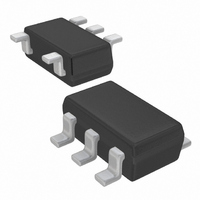
XC6108N26AMR-G Torex Semiconductor Ltd, XC6108N26AMR-G Datasheet

XC6108N26AMR-G
Specifications of XC6108N26AMR-G
Related parts for XC6108N26AMR-G
XC6108N26AMR-G Summary of contents
Page 1
XC6108 Series Voltage Detector with Separated Sense Pin & Delay Capacitor Pin ■GENERAL DESCRIPTION The XC6108 series is highly precise, low power consumption voltage detector, manufactured using CMOS and laser trimming technologies. Since the sense pin is separated from power ...
Page 2
XC6108 Series ■PIN CONFIGURATION USP-4 (BOTTOM VIEW the XC6108xxxA/B series, the dissipation pad should not be short-circuited with other pins the XC6108xxxC/D series, when the dissipation pad is short-circuited with other pins, connect it to the ...
Page 3
DIAGRAMS (1) XC6108CxxA (2) XC6108CxxB (3) XC6108NxxA (4) XC6108NxxB *The delay capacitance pin (Cd) is not connected to the circuit in the block diagram of XC6108CxxC (semi-custom). *The delay capacitance pin (Cd) is not connected to the circuit in ...
Page 4
XC6108 Series ■ABSOLUTE MAXIMUM RATINGS ●XC6108xxxA/B PARAMETER Input Voltage Output Current XC6108C Output Voltage XC6108N Sense Pin Voltage Delay Capacitance Pin Voltage Delay Capacitance Pin Current USP-4 Power Dissipation SOT-25 Operating Temperature Range Storage Temperature Range ●XC6108xxxC/D PARAMETER Input Voltage ...
Page 5
CHARACTERISTICS ●XC6108xxxA PARAMETER SYMBOL Operating Voltage Detect Voltage V Hysteresis Width V Detect Voltage ΔV Line Regulation (ΔV (*2) Supply Current 1 I (*2) Supply Current OUT1 (*3) Output Current I OUT2 CMOS Leakage Output I ...
Page 6
XC6108 Series ■ELECTRICAL CHARACTERISTICS (Continued) ●XC6108xxxB PARAMETER SYMBOL Operating Voltage Detect Voltage Hysteresis Width Detect Voltage ΔV Line Regulation (ΔV (*2) Supply Current 1 (*2) Supply Current 2 I (*3) Output Current I CMOS Leakage Output Current Nch Open Drain ...
Page 7
CHARACTERISTICS (Continued) ●XC6108xxxC PARAMETER SYMBOL Operating Voltage Detect Voltage V Hysteresis Width V Detect Voltage ΔV Line Regulation (ΔV (*2) Supply Current 1 I (*2) Supply Current OUT1 (*3) Output Current I OUT2 CMOS Leakage Output ...
Page 8
XC6108 Series ■ELECTRICAL CHARACTERISTICS (Continued) ●XC6108xxxD PARAMETER SYMBOL Operating Voltage Detect Voltage Hysteresis Width V Detect Voltage ΔV Line Regulation (ΔV (*2) Supply Current 1 (*2) Supply Current 2 I (*3) Output Current I CMOS Leakage Output Current Nch Open ...
Page 9
CHART SYMBOL E-1 NOMINAL DETECT DETECT VOLTAGE VOLTAGE ( DF(T) (V) MIN. 0.8 0.770 0.9 0.870 1.0 0.970 1.1 1.070 1.2 1.170 1.3 1.270 1.4 1.370 1.5 1.470 1.6 1.568 1.7 1.666 1.8 1.764 1.9 1.862 ...
Page 10
XC6108 Series ■TEST CIRCUITS Circuit 1 XC6108 Series Circuit 2 XC6108 Series Circuit 3 XC6108 Series Circuit 4 XC6108 Series Circuit 5 XC6108 Series 10/22 R=100kΩ (No resistor needed for CMOS output products) ...
Page 11
CIRCUITS (Continued) Circuit 6 Circuit 7 Circuit 8 XC6108 Series Circuit 9 *No delay capacitance pin available in the XC6108xxxC/D series. XC6108 Series (No resistor needed for CMOS output products) XC6108 Series (No resistor needed for CMOS output products) ...
Page 12
XC6108 Series ■OPERATIONAL EXPLANATION A typical circuit example is shown in Figure 1, and the timing chart of Figure 1 is shown in Figure 2 on page 14. ① early state, the sense pin is applied sufficiently high ...
Page 13
EXPLANATION (Continued) ●Function Chart V Cd SEN *1: V transits from condition ① to ② because of the combination of V OUT ●Example ex ranges from ‘L’ ...
Page 14
XC6108 Series ■OPERATIONAL EXPLANATION (Continued) Figure 1: Typical application circuit example V IN R SEN V SEN SEN Figure 2: The timing chart of Figure 1 14/ ...
Page 15
ON USE 1. Use this IC within the stated maximum ratings. Operation beyond these limits may cause degrading or permanent damage to the device. 2. The power supply input pin voltage drops by the resistance between power supply and ...
Page 16
XC6108 Series ■TYPICAL PERFORMANCE CHARACTERISTICS (1) Supply Current vs. Sense Voltage XC6108C25A GR 2.0 1.5 1.0 0.5 0 Sense Voltage : VSEN (V) Sense V oltage: V SEN (V ) (2) Supply Current vs. Input Voltage ...
Page 17
PERFORMANCE CHARACTERISTICS (Continued) (5) Hysteresis Voltage vs. Ambient Temperature XC6108C25AGR 0.20 0.15 0.10 0.05 -50 - Ambient Temperature : Ta (℃) A mbient Temperature ℃ ) (7) Output Voltage vs. Sense Voltage XC6108C25A GR 7.0 ...
Page 18
XC6108 Series ■TYPICAL PERFORMANCE CHARACTERISTICS (Continued) (10) Delay Resistance vs. Ambient Temperature XC6108C25AGR V SEN=6.0V V CD=0.0V V IN=5.0V 4 3.5 3 2.5 2 1.5 1 -50 - Ambient Temperature : Ta (℃) Ambient Temperature ℃ ...
Page 19
INFORMATION ●USP-4 * Soldering fillet surface is not formed because the sides of the pins are plated. ●SOT-25 2.9±0.2 +0.1 0.4 -0. (0.95) 1.9±0.2 0~0.1 +0.1 0.15 -0.05 XC6108 Series 19/22 ...
Page 20
XC6108 Series ■PACKAGING INFORMATION (Continued) ●USP-4 Reference Pattern Layout 20/22 ●USP-4 Reference Metal Mask Design ...
Page 21
RULE ●SOT-25 ① represents output configuration and integer number of detect voltage CMOS Output (XC6108C Series ① ② ③ ④ SOT-25 (TOP VIEW) ② represents decimal number of detect voltage (ex.) ③ represents options ...
Page 22
... Should you wish to use the products under conditions exceeding the specifications, please consult us or our representatives assume no responsibility for damage or loss due to abnormal use. 7. All rights reserved. No part of this datasheet may be copied or reproduced without the prior permission of TOREX SEMICONDUCTOR LTD. 22/22 ...


