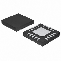
MAX6796TPLD4+T Maxim Integrated Products, MAX6796TPLD4+T Datasheet - Page 19

MAX6796TPLD4+T
Manufacturer Part Number
MAX6796TPLD4+T
Description
IC REG LIN W/SPR VSR 20-TQFN
Manufacturer
Maxim Integrated Products
Type
Regulator/Supervisorr
Datasheet
1.MAX6796TPLD2T.pdf
(25 pages)
Specifications of MAX6796TPLD4+T
Number Of Voltages Monitored
1
Output
Push-Pull, Totem Pole
Reset
Active Low
Reset Timeout
140 ms Minimum
Voltage - Threshold
4.625V
Operating Temperature
-40°C ~ 125°C
Mounting Type
Surface Mount
Package / Case
20-TQFN Exposed Pad
Number Of Outputs
1
Polarity
Positive
Input Voltage Max
72 V
Output Voltage
1.8 V to 11 V, 5 V
Output Type
Adjustable, Fixed
Dropout Voltage (max)
0.13 V at 20 mA
Output Current
300 mA
Line Regulation
1 %
Load Regulation
2 %
Maximum Power Dissipation
2.6667 W
Maximum Operating Temperature
+ 125 C
Mounting Style
SMD/SMT
Minimum Operating Temperature
- 40 C
Lead Free Status / RoHS Status
Lead free / RoHS Compliant
watchdog re-enables immediately when any of these
conditions are removed (as long as the RESET is not
asserted). Note that the output current threshold limit
includes hysteresis so that output current must exceed
13.8mA (max) to reenable the watchdog timer.
For stable operation over the full temperature range
and with load currents up to 150mA, use a 10µF (min)
output capacitor with an ESR < 0.5Ω. To reduce noise
and improve load-transient response and power-supply
rejection, use larger output-capacitor values. Some
ceramic dielectrics exhibit large capacitance and ESR
variation with temperature. For these types of capaci-
tors (such as Z5U and Y5V), much higher-value capaci-
tors are required to maintain stability over the
temperaure range. With X7R dielectrics, a 10µF capaci-
tor should be sufficient at all operating temperatures.
To improve power-supply rejection and transient
response, increase the capacitor between IN and GND.
When V
bilities decline drastically. High-impedance CMOS-
logic inputs connected to RESET can drift to
undetermined voltages. This presents no problems in
most applications, since most µPs and other circuitry
do not operate with a supply voltage below 1V. In those
applications where RESET must be valid down to 0,
adding a pulldown resistor between RESET and GND
sinks any stray leakage currents, holding RESET low
(Figure 4). The value of the pulldown resistor is not criti-
cal; 100kΩ is large enough not to load RESET and
small enough to pull RESET to ground. Open-drain
RESET versions are not recommended for applications
requiring valid logic for V
The power-fail comparator has a typical input hystere-
sis of 0.5% (of V
tions where a power-supply line is being monitored
through an external resistive-divider (Figure 5). Figure 6
shows how to add hysteresis to the power-fail com-
parator. Select the ratio of R5 and R6 so PFI sees 1.23V
when V
PFO is an open-drain output, resistors R7 and R8 add
hysteresis. R7 typically is an order of magnitude
greater than R5 or R6. The current through R5 and R6
should be at least 10µA to ensure that the 100nA (max)
PFI input current does not shift the trip point. R7 should be
larger than 50kΩ to prevent it from loading down the PFO.
Ensuring a Valid
High-Voltage, Micropower, Single/Dual Linear
IN
IN
falls below 1V, RESET current-sinking capa-
falls to the desired trip point (V
Capacitor Selection and Regulator
TH
______________________________________________________________________________________
). This is sufficient for most applica-
Regulators with Supervisory Functions
IN
RESET Output Down to
down to 0.
Adding Hysteresis to PFI
TRIP
Stability
V
). Since
IN
= 0
Figure 4. Ensuring RESET Valid to V
Figure 5. Setting Power-Fail Comparator to Monitor V
Figure 6. Adding Hysteresis Power-Fail Comparator
R5
R6
R5
R6
PFI
PFI
R7
MAX6792
MAX6794
MAX6796
MAX6791
MAX6791
GND
GND
GND
V
IN
V
V
IN
IN
IN
IN
IN
IN
RESET
PFO
PFO
= 0V
V
TERM
V
TERM
R8
IN
19


