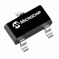
MCP1703T-3302E/CB Microchip Technology, MCP1703T-3302E/CB Datasheet - Page 4

MCP1703T-3302E/CB
Manufacturer Part Number
MCP1703T-3302E/CB
Description
IC REG LDO 3.3V 250MA SOT-23A
Manufacturer
Microchip Technology
Specifications of MCP1703T-3302E/CB
Package / Case
SOT-23A-3
Regulator Topology
Positive Fixed
Voltage - Output
3.3V
Voltage - Input
Up to 16V
Voltage - Dropout (typical)
0.525V @ 250mA
Number Of Regulators
1
Current - Output
250mA (Min)
Operating Temperature
-40°C ~ 125°C
Mounting Type
Surface Mount
Number Of Outputs
1
Polarity
Positive
Input Voltage Max
16 V
Output Voltage
3.3 V
Output Type
Fixed
Dropout Voltage (max)
0.65 V at 250 mA
Output Current
250 mA
Line Regulation
0.1 % / V
Load Regulation
1 %
Voltage Regulation Accuracy
2 %
Maximum Operating Temperature
+ 125 C
Mounting Style
SMD/SMT
Minimum Operating Temperature
- 40 C
Lead Free Status / RoHS Status
Lead free / RoHS Compliant
Current - Limit (min)
-
Lead Free Status / Rohs Status
Lead free / RoHS Compliant
Other names
MCP1703T-3302E/CBTR
Available stocks
Company
Part Number
Manufacturer
Quantity
Price
Company:
Part Number:
MCP1703T-3302E/CB
Manufacturer:
MICROCHIP
Quantity:
45 000
Company:
Part Number:
MCP1703T-3302E/CB
Manufacturer:
MICROCHIP
Quantity:
180
Part Number:
MCP1703T-3302E/CB
Manufacturer:
MICROCHIP/微芯
Quantity:
20 000
MCP1703
DC CHARACTERISTICS (CONTINUED)
TEMPERATURE SPECIFICATIONS
DS22049E-page 4
Electrical Specifications: Unless otherwise specified, all limits are established for V
I
Boldface type applies for junction temperatures, T
Dropout Voltage
Note
Output Delay Time
Output Noise
Power Supply Ripple
Rejection Ratio
Thermal Shutdown Protection
Note 1:
Temperature Ranges
Operating Junction Temperature Range
Maximum Junction Temperature
Storage Temperature Range
Thermal Package Resistance
Thermal Resistance, 3LD SOT-223
Thermal Resistance, 3LD SOT-23A
Thermal Resistance, 3LD SOT-89
Thermal Resistance, 8LD 2x3 DFN
LOAD
Note 1: The maximum allowable power dissipation is a function of ambient temperature, the maximum allowable junction
1,
= 100 µA, C
2:
3:
4:
5:
6:
7:
Note 5
Parameters
2: Thermal Resistance values are subject to change. Please visit the Microchip web site for the latest packaging
The minimum V
V
The input voltage V
TCV
temperature range. V
Load regulation is measured at a constant junction temperature using low duty cycle pulse testing. Changes in output
voltage due to heating effects are determined using thermal regulation specification TCV
Dropout voltage is defined as the input to output differential at which the output voltage drops 2% below its measured
value with an applied input voltage of V
The maximum allowable power dissipation is a function of ambient temperature, the maximum allowable junction
temperature and the thermal resistance from junction to air (i.e., T
dissipation will cause the device operating junction temperature to exceed the maximum 150°C rating. Sustained
junction temperatures above 150°C can impact the device reliability.
The junction temperature is approximated by soaking the device under test at an ambient temperature equal to the
desired Junction temperature. The test time is small enough such that the rise in the Junction temperature over the
ambient temperature is not significant.
temperature and the thermal resistance from junction to air (i.e., T
dissipation will cause the device operating junction temperature to exceed the maximum 150°C rating. Sustained
junction temperatures above 150°C can impact the device reliability.
information.
R
Parameters
is the nominal regulator output voltage. For example: V
OUT
OUT
= (V
= 1 µF (X7R), C
OUT-HIGH
IN
must meet two conditions: V
IN
(Note
V
OUT-LOW
= V
Symbol
DROPOUT
- V
T
PSRR
DELAY
T
e
OUT(MAX)
OUT-LOW
SD
2)
IN
N
= 1 µF (X7R), T
= lowest voltage measured over the temperature range.
Sym
) *10
T
T
T
+ V
JA
JC
JA
JC
JA
JC
JA
JC
A
J
J
Min
J
DROPOUT(MAX)
—
—
—
—
—
—
—
—
—
6
OUT(MAX)
(Note
/ (V
(1)
R
A
Min
-40
-65
—
—
—
—
—
—
—
—
—
* Temperature), V
7) of -40°C to +125°C.
= +25°C.
IN
1000
Typ
330
525
625
750
150
2.7V and V
+ V
44
—
8
DROPOUT(MAX)
or Vi
153,3
Typ
336
110
100
62
15
93
26
—
—
—
IN
R
1100
Max
650
725
975
—
—
—
—
= 1.2V, 1.5V, 1.8V, 2.5V, 2.8V, 3.0V, 3.3V, 4.0V, or 5.0V.
= 2.7V (whichever is greater); I
IN
+125
+150
+150
Max
(V
OUT-HIGH
—
—
—
—
—
—
—
—
A
A
, T
or 2.7V, whichever is greater.
, T
µV/(Hz)
OUT(MAX)
J
J
,
,
Units
mV
mV
mV
mV
mV
dB
µs
°C
JA
IN
Units
JA
°C/W
°C/W
°C/W
°C/W
= highest voltage measured over the
). Exceeding the maximum allowable power
°C
°C
°C
= V
). Exceeding the maximum allowable power
1/2
OUT(MAX)
+ V
I
I
I
I
V
Current Parameter
V
I
f = 100 Hz, C
V
V
Steady State
Transient
EIA/JEDEC JESD51-7
FR-4 0.063 4-Layer Board
EIA/JEDEC JESD51-7
FR-4 0.063 4-Layer Board
EIA/JEDEC JESD51-7
FR-4 0.063 4-Layer Board
EIA/JEDEC JESD51-7
FR-4 0.063 4-Layer Board
L
L
L
L
R
L
DROPOUT(MAX)
R
IN
INAC
R
= 250 mA, V
= 250 mA, 3.3V V
= 250 mA, 2.8V V
= 250 mA, 2.5V V
L
= 50 mA, f = 1 kHz, C
= 1.2V
< 2.5V, See Maximum Output
= 0V to 6V, V
= 50 resistive
2010 Microchip Technology Inc.
= 100 mV pk-pk, C
+ V
OUT
OUT
DROPOUT(MAX)
.
Conditions
OUT
Conditions
R
= 100 µA.
).
= 5.0V
OUT
= 1 µF, I
= 90% V
R
R
R
< 2.8V
OUT
< 5.0V
< 3.3V
,
IN
L
Note
= 100 µA,
= 0 µF,
= 1 µF
R
,
1,


