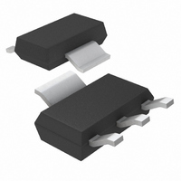
LT1175IST-5#PBF Linear Technology, LT1175IST-5#PBF Datasheet - Page 5

LT1175IST-5#PBF
Manufacturer Part Number
LT1175IST-5#PBF
Description
IC LDO REG NEG 5V 500MA SOT223-3
Manufacturer
Linear Technology
Datasheet
1.LT1175CN8-5PBF.pdf
(20 pages)
Specifications of LT1175IST-5#PBF
Regulator Topology
Negative Fixed
Voltage - Output
-5V
Voltage - Input
Down to -20V
Voltage - Dropout (typical)
0.5V @ 500mA
Number Of Regulators
1
Current - Output
500mA
Current - Limit (min)
Adjustable
Operating Temperature
-40°C ~ 85°C
Mounting Type
Surface Mount
Package / Case
SOT-223 (3 leads + Tab), SC-73, TO-261
Primary Input Voltage
20V
Output Voltage Fixed
5V
Dropout Voltage Vdo
500mV
No. Of Pins
3
Output Current
500mA
Operating Temperature Range
-40°C To +125°C
Msl
MSL 1 - Unlimited
Rohs Compliant
Yes
Lead Free Status / RoHS Status
Lead free by exemption / RoHS Compliant
Available stocks
Company
Part Number
Manufacturer
Quantity
Price
ELECTRICAL CHARACTERISTICS
temperature range, otherwise specifi cations are at T
To avoid confusion with “min” and “max” as applied to negative voltages, all voltages are shown as absolute values except where
polarity is not obvious.
PARAMETER
Current Limit (Note 12)
Line Regulation (Note 11)
Load Regulation (Note 6, 11)
Thermal Regulation
Output Voltage Temperature Drift
Note 1: Stresses beyond those listed under Absolute Maximum Ratings
may cause permanent damage to the device. Exposure to any Absolute
Maximum Rating condition for extended periods may affect device
reliability and lifetime.
Note 2: The LT1175 regulators are tested and specifi ed under pulse load
conditions such that T
at T
characterization and correlation with statistical process controls. The
LT1175I is guaranteed over the full –40°C to 125°C operating junction
temperature range. The LT1175MP is 100% tested and guaranteed over
the –55°C to 125°C operating junction temperature range.
Note 3: SHDN pin maximum positive voltage is 30V with respect to
– V
with respect to GND and –5V with respect to –V
Note 4: P
This power level holds only for input-to-output voltages up to 12V, beyond
which internal power limiting may reduce power. See Guaranteed Current
Limit curve in Typical Performance Characteristics section. Note that all
conditions must be met.
Note 5: GND pin current increases because of power transistor base
drive. At low input-to-output voltages (<1V) where the power transistor
is in saturation, GND pin current will be slightly higher. See Typical
Performance Characteristics.
Note 6: With I
increase higher than the 10μA to 25μA drawn by the output divider or fi xed
voltage SENSE pin, causing the output to rise above the regulated value.
To prevent this condition, an internal active pull-up will automatically turn
on, but supply current will increase.
IN
A
= 25°C. Performance at 0°C and 125°C is assured by design,
and 13.5V with respect to GND. Maximum negative voltage is –20V
MAX
= 1.5W for 8-pin packages, and 6W for 5-pin packages.
LOAD
= 0, at T
J
T
A
J
. The LT1175C is 100% production tested
> 125°C, power transistor leakage could
IN
.
CONDITIONS
V
I
I
I
V
I
P = 0 to P
T
LIM2
LIM4
LIM2
OUT
J
IN
IN
= 25°C to T
– V
– V
, I
= 0mA to 500mA
Open
Open
LIM4
A
OUT
OUT
= 25°C. V
MAX
= 1V to 12V
= 1V to V
Open
JMIN
(Notes 4, 9)
The
, or 25°C to T
l
OUT
IN
denotes specifi cations which apply over the full operating
= 20V
= 5V, V
Note 7: This is the current required to pull the output voltage to within 1V
of ground during shutdown.
Note 8: Dropout voltage is measured by setting the input voltage equal to
the normal regulated output voltage and measuring the difference between
V
pins tied to V
V
Note 9: Thermal regulation is a change in the output voltage caused by
die temperature gradients, so it is proportional to chip power dissipation.
Temperature gradients reach fi nal value in less than 100ms. Output voltage
changes after 100ms are due to absolute die temperature changes and
reference voltage temperature coeffi cient.
Note 10: The lower limit of 0.8V is guaranteed to keep the regulator in
shutdown. The upper limit of 2.5V is guaranteed to keep the regulator
active. Either polarity may be used, referenced to GND pin.
Note 11: Load and line regulation are measured on a pulse basis with
pulse width of 20ms or less to keep chip temperature constant. DC
regulation will be affected by thermal regulation (Note 8) and chip
temperature changes. Load regulation specifi cation also holds for currents
up to the specifi ed current limit when I
Note 12: Current limit is reduced for input-to-output voltage above 12V.
See the graph in Typical Performance Characteristics for guaranteed limits
above 12V.
Note 13: Operating at very large input-to-output differential voltages
(>15V) with load currents less than 5mA requires an output capacitor with
an ESR greater than 1Ω to prevent low level output oscillations.
IN
DO
and V
= 0.15 + 1.1Ω (I
JMAX
IN
= 7V, I
OUT
5-Pin Packages
8-Pin Packages
. For currents between 100mA and 500mA, with both I
IN
OUT
, maximum dropout can be calculated from
= 0, V
OUT
).
SHDN
= 3V, I
l
l
l
l
l
l
LIM2
LIM2
MIN
520
390
260
130
or I
and I
LIM4
0.003
0.04
0.25
TYP
800
600
400
200
0.1
0.1
LIM4
are left open.
tied to V
0.015
1300
LT1175
MAX
0.35
1.25
975
650
325
0.1
0.2
IN
.
LIM
UNITS
%/W
%/W
1175ff
5
%/V
mA
mA
mA
mA
%
%


