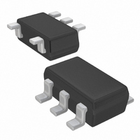
XC6222B281MR-G Torex Semiconductor Ltd, XC6222B281MR-G Datasheet - Page 8

XC6222B281MR-G
Manufacturer Part Number
XC6222B281MR-G
Description
IC REG LDO 2.8V SOT-25
Manufacturer
Torex Semiconductor Ltd
Datasheet
1.XC6222B28BMR-G.pdf
(26 pages)
Specifications of XC6222B281MR-G
Regulator Topology
Positive Fixed
Voltage - Output
2.8V
Voltage - Input
Up to 6V
Voltage - Dropout (typical)
0.16V @ 300mA
Number Of Regulators
1
Current - Output
700mA (Min)
Current - Limit (min)
720mA
Operating Temperature
-40°C ~ 85°C
Mounting Type
Surface Mount
Package / Case
SOT-23-5, SC-74A, SOT-25
Lead Free Status / RoHS Status
Lead free / RoHS Compliant
Other names
893-1141-2
■OPERATIONAL EXPLANATION
<Input and Output Capacitors>
The XC6222 needs an output capacitor C
the chart below. If a loss of the capacitance happens, stable phase compensation may not be obtained. Please ensure to
use a capacitor which does not depend on bias or temperature too much. For a stable power input, please connect an input
capacitor C
<Reverse Current Protection>
The XC6222 series includes reverse current protection to prevent the damage to any connected products such as batteries as a
result of current flow from the V
suppress the reverse current to 1.5μA (MAX.). When V
pin to the V
to the CE pin, the sink current of the V
level signal is inputted to the CE pin, the sink current of the V
which may result in the IC being damaged. In this case, please do not connect a power supply to the V
from V
adding a power supply or battery, a low level signal should be input to the CE pin for chip disable in order to protect a reverse
current at V
Example) The voltage less than V
8/26
The voltage divided by two resistors R1 and R2 is compared with the internal reference voltage by the error amplifier. The
P-channel MOSFET connected to the V
pin is controlled and stabilized by a system of negative feedback. The current limit and short protection operate in relation to
the level of output current. The thermal protection operates in relation to the level of heat generation. The reverse current
protection operates when V
pin's signal.
●Output Capacitor (C
Please also note when the XC6222A/C series connects external power supply to the V
OUTPUT VOLTAGE (V)
VIN
CE
XC6222
OUT(E)
0.8V~2.05V
2.1V~2.45V
2.5V~5.0V
IN
SS
IN
(actual output voltage value)or more to 6.0V or less. When the voltage less than V
< V
of 1.0μF between the V
pin is 95μA (TYP.) as the IC operation current. With the XC6222A/C series, when a low level signal is inputted
ThermalShutdown
ON/OFF
Control
CurrentLimit
OUT
Protection
Reverce
Current
XC6222Aseries
.
&
circuit
each
L
Series
) Table
Error
OUT
Amp
OUT(E)
+
-
Reference
OUT
voltage is higher than V
Voltage
CFB
(actual output voltage value) is applied to the V
pin to the V
OUTPUT CAPACITOR VALUE
IN
OUT
OUT
R1
pin and the V
L
R2
C
C
C
pin is minimized to 2.8μA (TYP.). However, with the XC6222B/D series, when a low
for phase compensation. Values required for the phase compensation are shown in
L
L
L
pin, is then driven by the subsequent output signal. The output voltage at the V
=6.8μF (MIN.)
=4.7μF (MIN.)
=2.2μF (MIN.)
IN
VOUT
VSS
pin. When V
SS
IN
pin.
voltage. Further, the IC's internal circuitry can be turned off via the CE
IN
is smaller then V
OUT
IN
is smaller than V
* When the CE pin is connected to the V
from the step-up DC/DC goes through to the V
current up to around 150mA if the USB connection is removed from
the V
when the USB connection is removed from the V
pin goes through the C
IN
pin (V
IN
OUT
OUT
< V
pin as "OR" connection.
, the V
OUT
OUT,
). CE pin voltage should be maintained low
the reverse current protection works and
OUT
L
OUT
pin sink current flows from the V
auto discharge circuit to the V
pin, please use it within the range
OUT(E)
IN
pin, an output voltage 2.8V
is applied to the V
IN
OUT
pin as reverse
IN
pin.
pin.
OUT
pin by
SS
OUT
OUT
pin


