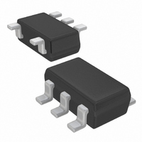
XC6222B331MR-G Torex Semiconductor Ltd, XC6222B331MR-G Datasheet - Page 5

XC6222B331MR-G
Manufacturer Part Number
XC6222B331MR-G
Description
IC REG LDO 3.3V SOT-25
Manufacturer
Torex Semiconductor Ltd
Datasheet
1.XC6222B28BMR-G.pdf
(26 pages)
Specifications of XC6222B331MR-G
Regulator Topology
Positive Fixed
Voltage - Output
3.3V
Voltage - Input
Up to 6V
Voltage - Dropout (typical)
0.12V @ 300mA
Number Of Regulators
1
Current - Output
700mA (Min)
Current - Limit (min)
720mA
Operating Temperature
-40°C ~ 85°C
Mounting Type
Surface Mount
Package / Case
SOT-23-5, SC-74A, SOT-25
Lead Free Status / RoHS Status
Lead free / RoHS Compliant
Other names
893-1143-2
Available stocks
Company
Part Number
Manufacturer
Quantity
Price
Part Number:
XC6222B331MR-G
Manufacturer:
TOREX
Quantity:
20 000
■ELECTRICAL CHARACTERISTICS (Continued)
NOTE:
* 4: VOUT (T) is nominal output voltage
* 1: Unless otherwise stated, input voltage is VIN=VOUT(T)+1.0V.
* 2: VOUT (E) is effective output voltage (Refer to the voltage chart E-0 and E-1)
* 3: The relation between VOU T (E) and VOUT (T) is shown in the voltage chart E-0 and E-1.
* 5: Vdif = {VIN1
* 6: VOUT1 equals 98% of the output voltage when amply stabilized VOUT (T) +1.0V are supplied to the V
* 7: VIN1 is the input voltage when VOUT1 appears at the V
* 8: Reverse current (I
* 9: V
*10: For the XC6222A/C series only. In the XC6222B/D series, the current flows from the V
*11: For the XC6222B/D series only. The XC6222A/C series discharges via two resistors R1 and R2 shown in the block diagram.
It is defined as output voltages when an amply stabilized VOUT (T) +1.0V is supplied to the VIN pin while maintaining a certain
IOUT .
when CE pin is low. Please do not connect another power supply to the V
connects external power supply to the V
6.0V or less. When the voltage less than V
should be input to the CE pin for chip disable in order to protect a reverse current at V
OUT
pin sink current (I
(*7)
-VOUT1
REV
) flows from V
REVS
(*6)
}
) flows from V
OUT
to V
OUT
OUT
IN
to V
.
OUT(E)
pin, please use it within the range from V
SS
.
is applied to the V
OUT
pin while input voltage is gradually decreased.
OUT
pin by adding a power supply or battery, a low level signal
OUT
pin. Please also note when the XC6222A/C series
IN
OUT(E)
< V
OUT
OUT
pin to the V
(actual output voltage value)or more to
.
IN
SS
pin.
pin via the internal switch
XC6222
Series
5/26


