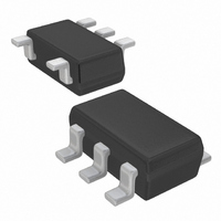
XC6216C202MR-G Torex Semiconductor Ltd, XC6216C202MR-G Datasheet - Page 21

XC6216C202MR-G
Manufacturer Part Number
XC6216C202MR-G
Description
IC REG LDO 2V SOT-25
Manufacturer
Torex Semiconductor Ltd
Datasheet
1.XC6216C202MR-G.pdf
(43 pages)
Specifications of XC6216C202MR-G
Regulator Topology
Positive Fixed
Voltage - Output
2V
Voltage - Input
Up to 28V
Voltage - Dropout (typical)
1.9V @ 100mA
Number Of Regulators
1
Current - Output
100mA (Min)
Operating Temperature
-40°C ~ 85°C
Mounting Type
Surface Mount
Package / Case
SOT-23-5, SC-74A, SOT-25
Lead Free Status / RoHS Status
Lead free / RoHS Compliant
Current - Limit (min)
-
Other names
893-1079-2
Available stocks
Company
Part Number
Manufacturer
Quantity
Price
■ NOTES ON USE
5. Torex places an importance on improving our products and its reliability.
1. Please use this IC within the stated absolute maximum ratings. The IC is liable to malfunction should the ratings be
2. Where wiring impedance is high, operations may become unstable due to the noise and/or phase lag depending on output
3. Phase compensation inside the IC is performed in the XC6216/XE6216 series. Therefore, an abnormal oscillation does not
4. Notes on setting output voltage externally (C type) Ta=25℃
However, by any possibility, we would request user fail-safe design and post-aging treatment on system or equipment.
●Setting Resistance-Dependant of XC6216 Series’ Output Voltage
The output voltage can be set externally by the following equation:
If the equation (3) is assigned to the equation (2), the equation becomes as below:
For this, the following equation can be used for setting output voltage externally:
And the equation (4) will be;
The second term of the equation (6), R
The I
The cause of the output accuracy error, R
Accordingly, if R
exceeded.
current. Please strengthen V
occur even if there is no output capacitor C
(V
over shoot, which occurs because of the load change can be controlled by placing the output capacitor C
0.1uF~1.0uF between the V
placed to the IC as close as possible with a shorter wiring.
IN
FB
) and the ground pin (V
can be calculated by the following equation:
I
I
I
V
V
V
I
R
21
22
21
FB
OUT
OUT
OUT
21
=I
=2.0V/R
=I
=2.0V / R
・
FB
FB
I
=2.0V
=2.0V+R
=2.0V+R
=2.0V+R
FB
21
+I
+2.0V/R
=2.0V
=R
<< R
22
21
22
・
・
FB
FB
(R
・
21
21
2.0V/ R
, the output voltage error becomes minute.
21
22
21
R
・
・
21
・
+ R
I
I
21
21
(I
/ R
SS
FB
OUT
22
) is required for input stability. Also, the output voltage fluctuation such as under shoot or
FB
IN
FB
+2.0V/R
) / R
and V
pin and V
22
21
+ R
・
SS
22
21
I
)
・
21
FB
wiring in particular.
・
, is the cause of the output accuracy error.
I
SS
FB
L
. An input capacitor C
I
FB
can be calculated by the equation below;
pin. The input capacitor (C
………………………………………………………………………
………………………………………………………………………
………………………………………………………………………
………………………………………………………………………
………………………………………………………………………
………………………………………………………………………
………………………………………………………………………
………………………………………………………………………
………………………………………………………………………
IN
around 0.1uF~1.0uF between the power input pin
IN
) and the output capacitor (C
XC6216/XE6216
L
) should be
L
21/43
Series
around
(1)
(2)
(3)
(4)
(5)
(6)
(7)


