SC553ISKTRT Semtech, SC553ISKTRT Datasheet - Page 5
SC553ISKTRT
Manufacturer Part Number
SC553ISKTRT
Description
IC LDO ADJ REG 150MA SOT-23-5
Manufacturer
Semtech
Datasheet
1.SC553ISKTRT.pdf
(7 pages)
Specifications of SC553ISKTRT
Regulator Topology
Positive Adjustable
Voltage - Output
1.25 ~ 6 V
Voltage - Input
2.25 ~ 6.5 V
Voltage - Dropout (typical)
0.15V @ 150mA
Number Of Regulators
1
Current - Output
150mA
Current - Limit (min)
400mA
Operating Temperature
-40°C ~ 85°C
Mounting Type
Surface Mount
Package / Case
SOT-23-5, SC-74A, SOT-25
Lead Free Status / RoHS Status
Lead free / RoHS Compliant
Other names
SC553ISKTR
Available stocks
Company
Part Number
Manufacturer
Quantity
Price

Part Number:
SC553ISKTRT
Manufacturer:
SEMTECH/美国升特
Quantity:
20 000


Theory Of Operation
The SC553 is intended for applications where very low
dropout voltage, low supply current and low output noise
are critical. It provides a very simple, low cost solution
that uses very little pcb real estate. Only two external
capacitors are required for operation.
The SC553 contains a bandgap reference trimmed for
optimal temperature coefficient which is fed into the
inverting input of an error amplifier. The output voltage
of the regulator is divided down externally using a
resistor divider and compared to the bandgap voltage
via the adjust pin (ADJ). The error amplifier drives the
gate of a low R
maintain V
An active high enable pin (EN) allows the regulator to be
shut down. Pulling this pin low causes the device to
enter a very low power shutdown mode, where it will draw
typically 0.1µA from the input supply.
The regulator has its own current limit circuitry to
ensure that the output current will not damage the
device during output short, overload or start-up. The
current limit is guaranteed to be greater than 400mA to
allow fast charging of the output capacitor and high
initial currents for DSP initialization.
The SC553 includes thermal shutdown circuitry to turn
off the device if T
device remaining off until T
Reverse battery protection circuitry ensures that the
device cannot be damaged if the input supply is
accidentally reversed, limiting the reverse current to less
than 1.5mA.
POWER MANAGEMENT
Marking Information
Applications Information
2004 Semtech Corp.
OUT
such that V
DS(ON)
J
exceeds 150°C (typical), with the
P-channel MOSFET pass device to
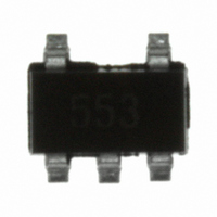
553
Top Mark
ADJ
= V
J
drops by 15°C (typical).
REF
NOT RECOMMENDED FOR NEW DESIGN
.
5
Component Selection - General
Output capacitor - Semtech recommends a minimum
capacitance of 1µF at the output with an equivalent
series resistance (ESR) of < 1
the SC553 has been designed to be used with ceramic
capacitors, it does not have to be used with ceramic
capacitors, allowing the designer a choice. Increasing the
bulk capacitance will further reduce output noise and
improve the overall transient response.
Input capacitor - Semtech recommends the use of a
1µF ceramic capacitor at the input. This allows for the
device being some distance from any bulk capacitance
on the rail. Additionally, input droop due to load transients
is reduced, improving overall load transient response.
External voltage selection resistors - the use of 1%
resistors, and designing for a current flow
recommended to ensure a well regulated output (thus
R2
below) will be:
V
VIN
OUT
=
125k ). The output voltage (referring to Figure 1
. 1
C1
1uF
250
yyww = Datecode (Example: 0108)
•
1
+
1
3
R
R
U1
IN
EN
1
2
Bottom Mark
GND
2
yyww
Figure 1
SC553
OUT
ADJ
5
4
over temperature. While
R1
R2
www.semtech.com
SC553
10µA is
C2
1uF
VOUT
Related parts for SC553ISKTRT
Image
Part Number
Description
Manufacturer
Datasheet
Request
R

Part Number:
Description:
SC55-10-3956-10 2.2UH
Manufacturer:
Tyco Electronics
Datasheet:

Part Number:
Description:
EVALUATION BOARD
Manufacturer:
Semtech
Datasheet:
Part Number:
Description:
EVALUATION BOARD
Manufacturer:
Semtech
Datasheet:
Part Number:
Description:
VOLTAGE SUPPRESSOR, TRANSIENT SEMTECH
Manufacturer:
Semtech
Datasheet:

Part Number:
Description:
HIGH VOLTAGE CAPACITORS MONOLITHIC CERAMIC TYPE
Manufacturer:
Semtech Corporation
Datasheet:
Part Number:
Description:
EZ1084CM5.0 AMP POSITIVE VOLTAGE REGULATOR
Manufacturer:
Semtech Corporation
Datasheet:
Part Number:
Description:
3.0 AMP LOW DROPOUT POSITIVE VOLTAGE REGULATORS
Manufacturer:
Semtech Corporation
Datasheet:
Part Number:
Description:
Manufacturer:
Semtech Corporation
Datasheet:
Part Number:
Description:
RailClamp Low Capacitance TVS Diode Array
Manufacturer:
Semtech Corporation
Datasheet:
Part Number:
Description:
Manufacturer:
Semtech Corporation
Datasheet:
Part Number:
Description:
Manufacturer:
Semtech Corporation
Datasheet:
Part Number:
Description:
Manufacturer:
Semtech Corporation
Datasheet: