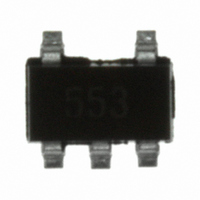
SC553ISKTRT Semtech, SC553ISKTRT Datasheet - Page 6

SC553ISKTRT
Manufacturer Part Number
SC553ISKTRT
Description
IC LDO ADJ REG 150MA SOT-23-5
Manufacturer
Semtech
Datasheet
1.SC553ISKTRT.pdf
(7 pages)
Specifications of SC553ISKTRT
Regulator Topology
Positive Adjustable
Voltage - Output
1.25 ~ 6 V
Voltage - Input
2.25 ~ 6.5 V
Voltage - Dropout (typical)
0.15V @ 150mA
Number Of Regulators
1
Current - Output
150mA
Current - Limit (min)
400mA
Operating Temperature
-40°C ~ 85°C
Mounting Type
Surface Mount
Package / Case
SOT-23-5, SC-74A, SOT-25
Lead Free Status / RoHS Status
Lead free / RoHS Compliant
Other names
SC553ISKTR
Available stocks
Company
Part Number
Manufacturer
Quantity
Price
Part Number:
SC553ISKTRT
Manufacturer:
SEMTECH/美国升特
Quantity:
20 000
Thermal Considerations
The worst-case power dissipation for this part is given
by:
For all practical purposes, equation (1) can be reduced
to the following expression:
Looking at a typical application, 3.3V to 2.8V at 150mA:
V
V
I
T
Inserting these values into equation (2) gives us:
Using this figure, we can calculate the maximum thermal
impedance allowable to maintain T
With the standard SOT-23-5 Land Pattern shown at the
end of this datasheet, and minimum trace widths, the
thermal impedance junction to ambient for SC553 is
256°C/W. Thus no additional heatsinking is required for
this example.
The junction temperature can be reduced further (or
higher power dissipation can be allowed) by the use of
larger trace widths and connecting PCB copper to the
GND pin (pin 2), which connects directly to the device
substrate. Adding approximately one square inch of PCB
copper to pin 2 will reduce
130°C/W and T
approximately 100°C. The use of multi layer boards with
internal ground/power planes will lower the junction
temperature and improve overall output voltage
accuracy.
POWER MANAGEMENT
P
θ
OUT
Applications Information (Cont.)
A
IN(MAX)
OUT(MIN)
D
JA
(
2004 Semtech Corp.
= 85°C
MAX
(
MAX
= 150mA
)
)
= 3.3 + 5% = 3.465V
=
= 2.8V - 2% = 2.744V
=
(
V
(
T
IN
( J
(
MAX
MAX
P
)
)
D
−
(
−
MAX
V
T
OUT
A
J(MAX)
)
(
MAX
(
MIN
)
)
)
for the example above to
=
)
•
(
I
125
OUT
. 0
(
108
MAX
−
NOT RECOMMENDED FOR NEW DESIGN
85
)
JA
J
+
)
V
to approximately
=
125°C:
IN
370
(
MAX
°
)
C
•
I
/
Q
W
(
MAX
)
(1)
(2)
6
Layout Considerations
While layout for linear devices is generally not as critical
as for a switching application, careful attention to detail
will ensure reliable operation.
1) Attaching the part to a larger copper footprint will
enable better heat transfer from the device, especially
on PCBs where there are internal ground and power
planes.
2) Place the input and output capacitors close to the
device for optimal transient response and device
behaviour.
3) While the external resistor divider does not need to be
close to the device, care should be taken to avoid routing
the connections next to any lines carrying large amounts
of noise. The simplest solution is to place these resistors
close to the device and routing the top of R1 to the load
if not adjacent to the part.
4) Connect all ground connections directly to the ground
plane. If there is no ground plane, connect to a common
local ground point before connecting to board ground.
Typical Characteristics
250
225
200
175
150
125
100
75
50
25
0
2.0
T
A
Dropout Voltage vs. Output Voltage
= 25°C
2.5
3.0
vs. Output Current
3.5
Top to bottom:
I
I
I
OUT
OUT
OUT
V
= 150mA
= 100mA
= 50mA
OUT
4.0
(V)
4.5
www.semtech.com
5.0
SC553
5.5
6.0


