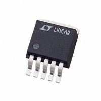
LT1185CQ#TR Linear Technology, LT1185CQ#TR Datasheet

LT1185CQ#TR
Specifications of LT1185CQ#TR
Available stocks
Related parts for LT1185CQ#TR
LT1185CQ#TR Summary of contents
Page 1
... The LT1185 has all the protection features of previous LTC regulators, including power limiting and thermal shutdown. , LT, LTC and LTM are registered trademarks of Linear Technology Corporation. All other trademarks are the property of their respective owners. 1.6 + 1.4 2 ...
Page 2
LT1185 ABSOLUTE AXI U RATI GS Input Voltage .......................................................... 35V Input-Output Differential ......................................... 30V FB Voltage ................................................................ 7V REF Voltage .............................................................. 7V Output Voltage ........................................................ 30V Output Reverse Voltage ............................................ 2V Operating Ambient Temperature Range LT1185C ............................................... ...
Page 3
ELECTRICAL CHARACTERISTICS The ● denotes specifications which apply over the operating temperature range, otherwise specifications are at T Adjustable version 7.4V 5V OUT PARAMETER Load Regulation (Note 7) Line Regulation (Note 7) Minimum Input ...
Page 4
LT1185 W U TYPICAL PERFOR A CE CHARACTERISTICS Internal Current Limit 5 4 GUARANTEED LIMIT 3 TYPICAL 2 GUARANTEED 1 LIMIT TEST POINTS INPUT-OUTPUT DIFFERENTIAL (V) LT1185 • TPC01 Ground Pin Current 160 ...
Page 5
U U APPLICATIO S I FOR ATIO Block Diagram A simplified block diagram of the LT1185 is shown in Figure 1. A 2.37V bandgap reference is used to bias the input of the error amplifier A1, and the reference amplifier ...
Page 6
LT1185 U U APPLICATIO S I FOR ATIO Amplifier A2 is used to generate an internal current through Q4 when an external resistor is connected from the REF pin to ground. This current is equal to 2.37V divided by R ...
Page 7
U U APPLICATIO S I FOR ATIO Large output capacitors (electrolytic or solid tantalum) will not cause the LT1185 to oscillate, but they will cause a damped “ringing” at light load currents where the ESR of the capacitor is several ...
Page 8
LT1185 U U APPLICATIO S I FOR ATIO factor is that local ambient temperature may be somewhat higher because of the point source of heat. The conse- quences of excess junction temperature include poor reliability, especially for plastic packages, and ...
Page 9
U U APPLICATIO S I FOR ATIO for remote sense applications, they may need to be con- sidered. Ground lead resistance of 0.4Ω would cause an output voltage error (3A/40)(0.4Ω) = 30mV ...
Page 10
LT1185 U U APPLICATIO S I FOR ATIO Thermal Regulation IC regulators have a regulation term not found in discrete designs because the power transistor is thermally coupled to the reference. This creates a shift in the output voltage which ...
Page 11
U TYPICAL APPLICATIO 15k + 2µF 2N3906 V IN TANT GND REF – V LT1185 IN V OUT LT1185 • TA03a Auxiliary + 12V Low Dropout Regulator for Switching Supply PRIMARY *DIODE CONNECTION INDICATES A FLYBACK SWITCHING ...
Page 12
LT1185 U TYPICAL APPLICATIO 360k 2.2µF TANT V IN REF R4** 1k R5* 0.01Ω – R6** 1k OPTIONAL HYSTERESIS 3 + LT1006 2 – Time Delayed Start-Up + R3** † ...
Page 13
W W SCHE ATIC DIAGRA LT1185 1185ff 13 ...
Page 14
LT1185 PACKAGE DESCRIPTIO .320 – .350 (19.30 – 19.69) (8.13 – 8.89) .420 – .480 (10.67 – 12.19) .390 – .415 (9.906 – 10.541) .230 – .270 (5.842 – 6.858) .460 – .500 (11.684 – 12.700) .330 – .370 (8.382 ...
Page 15
... DIMENSIONS IN INCH/(MILLIMETER) 2. DRAWING NOT TO SCALE Information furnished by Linear Technology Corporation is believed to be accurate and reliable. However, no responsibility is assumed for its use. Linear Technology Corporation makes no represen- tation that the interconnection of circuits as described herein will not infringe on existing patent rights Package ...
Page 16
... Supply Current, Adjustable Current Limit For High Performance Microprocessors V : –0.9V to –20V 3µA, ThinSOT Package SD www.linear.com ● 1N4001 ADD FOR INDUCTIVE LOADS + C1 4.7µF V OUT TANT C3 0.05µF – = 5V, OUT = –1.21V 0.34V 30µA, OUT(MIN LT/LWI 0906 REV F • PRINTED IN USA © LINEAR TECHNOLOGY CORPORATION 1994 1185ff ...


