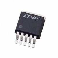
LT1185CQ#TR Linear Technology, LT1185CQ#TR Datasheet - Page 3

LT1185CQ#TR
Manufacturer Part Number
LT1185CQ#TR
Description
IC REG LDO ADJUSTABLE 3A DDPAK-5
Manufacturer
Linear Technology
Datasheet
1.LT1185CTPBF.pdf
(16 pages)
Specifications of LT1185CQ#TR
Regulator Topology
Negative Adjustable
Voltage - Output
-2.5 ~ -25 V
Voltage - Input
-4.2 ~ -35 V
Voltage - Dropout (typical)
0.67V @ 3A
Number Of Regulators
1
Current - Output
3A
Current - Limit (min)
Adjustable
Operating Temperature
0°C ~ 125°C
Mounting Type
Surface Mount
Package / Case
TO-263-5, D²Pak (5 leads + Tab), TO-263BA
Lead Free Status / RoHS Status
Contains lead / RoHS non-compliant
Available stocks
Company
Part Number
Manufacturer
Quantity
Price
ELECTRICAL CHARACTERISTICS
PARAMETER
Load Regulation (Note 7)
Line Regulation (Note 7)
Minimum Input Voltage
Internal Current Limit (See Graph for
Guaranteed Curve) (Note 12)
External Current Limit
Programming Constant
External Current Limit Error
Quiescent Supply Current
Supply Current Change with Load
REF Pin Shutoff Current
Thermal Regulation (See Applications
Information)
Reference Voltage Temperature Coefficient
Thermal Resistance Junction to Case
Note 1: Stresses beyond those listed under Absolute Maximum Ratings
may cause permanent damage to the device. Exposure to any Absolute
Maximum Rating condition for extended periods may affect device
reliability and lifetime.
Note 2: Reference voltage is guaranteed both at nominal conditions (no
load, 25°C) and at worst-case conditions of load, line, power and
temperature. An intermediate value can be calculated by adding the effects
of these variables in the actual application. See the Applications
Information section of this data sheet.
Note 3: Dropout voltage is tested by reducing input voltage until the
output drops 1% below its nominal value. Tests are done at 0.5A and 3A.
The power transistor looks basically like a pure resistance in this range so
that minimum differential at any intermediate current can be calculated by
interpolation; V
0.5A, see graph.
Note 4: “Minimum input voltage” is limited by base emitter voltage drive
of the power transistor section, not saturation as measured in Note 3. For
output voltages below 4V, “minimum input voltage” specification may limit
dropout voltage before transistor saturation limitation.
Note 5: Supply current is measured on the ground pin, and does not
include load current, R
The
Adjustable version, V
●
denotes specifications which apply over the operating temperature range, otherwise specifications are at T
DROPOUT
LIM
= 0.25V + 0.25Ω • I
IN
, or output divider current.
= 7.4V, V
OUT
= 5V, I
OUT
. For load current less than
OUT
CONDITIONS
I
V
V
I
I
1.5V ≤ V
V
V
V
5k ≤ R
(Note 11)
1A ≤ I
R
I
4V ≤ V
V
V
V
I
(Note 8)
TO-3 Control Area
Power Transistor
TO-220 Control Area
Power Transistor
OUT
OUT
OUT
OUT
OUT
IN
IN
IN
IN
IN
IN
IN
IN
LIM
= 1mA, R
– V
– V
– V
– V
– V
– V
– V
– V
= 5mA to 3A
= 1A (Note 4), V
= 3A
= 5mA, V
= 5mA to 2A
= 15k • A/I
LIM
LIM
IN
OUT
OUT
OUT
OUT
OUT
OUT
OUT
OUT
IN
≤ 25V (Note 5)
≤ 3A
≤ 15k, V
– V
= 1.5V to 10V, V
= 1V to 20V, V
= 15V
= 20V
= 30V
= V
≥ 2V
= 10V
LIM
OUT
OUT
SAT
LIM
= 4.02k, unless otherwise noted.
= V
≤ 10V
(Note 10)
OUT
OUT
REF
= 1V
= V
OUT
OUT
REF
Note 6: The 25W power level is guaranteed for an input-output voltage of
8.3V to 17V. At lower voltages the 3A limit applies, and at higher voltages
the internal power limiting may restrict regulator power below 25W. See
graphs.
Note 7: Line and load regulation are measured on a pulse basis with a
pulse width of ≈ 2ms, to minimize heating. DC regulation will be affected
by thermal regulation and temperature coefficient of the reference. See
Applications Information section for details.
Note 8: Guaranteed by design and correlation to other tests, but not
tested.
Note 9: T
the LT1185M. Power transistor area and control circuit area have different
maximum junction temperatures. Control area limits are T
the LT1185C and LT1185I and 150°C for the LT1185M. Power area limits
are 150°C for LT1185C and LT1185I and 175°C for LT1185M.
Note 10: V
0.25V + 0.25 • I
Note 11: Current limit is programmed with a resistor from REF pin to GND
pin. The value is 15k/I
Note 12: For V
other current limit tests.
= 5V
= 5V
JMIN
SAT
●
●
●
●
●
●
●
●
●
●
= 0°C for the LT1185C, – 40°C for LT1185I, and –55°C for
is the maximum specified dropout voltage;
IN
OUT
– V
.
OUT
LIM
MIN
3.3
3.1
2.0
1.0
0.2
0.4
= 1.5V; V
.
IN
0.02 I
0.04 I
= 5V, V
0.002
0.005
0.003
TYP
0.05
15k
4.0
4.3
3.6
3.0
1.7
0.4
2.5
25
10
2
LIM
LIM
OUT
0.06 I
0.09 I
= 3.5V. V
A
= 25°C.
0.014
MAX
0.01
LIM
LIM
0.01
0.3
4.2
4.4
4.2
2.6
1.0
3.5
40
25
7
1
3
1
3
OUT
LT1185
+ 0.03
+ 0.05
JMAX
= 1V for all
= 125°C for
UNITS
mA/A
mA/A
%/°C
°C/W
°C/W
°C/W
°C/W
%/W
1185ff
3
%/V
A•Ω
mA
µA
%
V
V
A
A
A
A
A
A
A


