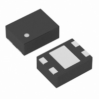
XC6221A252GR-G Torex Semiconductor Ltd, XC6221A252GR-G Datasheet - Page 8

XC6221A252GR-G
Manufacturer Part Number
XC6221A252GR-G
Description
IC REG LDO 2.5V .25A USP-4
Manufacturer
Torex Semiconductor Ltd
Datasheet
1.XC6221A332MR-G.pdf
(28 pages)
Specifications of XC6221A252GR-G
Regulator Topology
Positive Fixed
Voltage - Output
2.5V
Voltage - Input
Up to 6V
Voltage - Dropout (typical)
0.095V @ 100mA
Number Of Regulators
1
Current - Output
200mA (Min)
Current - Limit (min)
200mA
Operating Temperature
-40°C ~ 85°C
Mounting Type
Surface Mount
Package / Case
USP-4
Lead Free Status / RoHS Status
Lead free / RoHS Compliant
●Except USPN-4
●USPN-4
8/28
<C
<Input and Output Capacitors>
CE
■OPERATIONAL EXPLANATION
<Output Voltage Control>
The XC6221 needs an output capacitor C
shown in the chart below. If a loss of the capacitance happens, the stable phase compensation may not be obtained.
Please ensure to use a capacitor which does not depend on bias or temperature too much. For a stable power input,
please connect an input capacitor C
L
OUTPUT VOLTAGE (V)
OUTPUT VOLTAGE (V)
where
XC6221B/D series can discharge the electric charge in the output capacitor (C
enables the whole IC circuit to be turned off, is inputted via the N-channel transistor and C
(R
value is set at 780Ω(V
auto-discharge resistance (R
resistance value [R
the N-channel transistor is calculated by the following formula.
Auto-Discharge Function>
XC6221
The voltage divided by resistors R1 & R2 is compared with the internal reference voltage by the error amplifier. The
P-channel MOSFET connected to the V
V
operate in relation to the level of output current. Further, the IC's internal circuitry can be shutdown via the CE pin's signal.
τ: C
V : Output voltage after discharge
V
t : Discharge time
DCHG
OUT
OUT (E)
V = V
0.80V~1.15V
1.20V~1.35V
1.40V~4.00V
4.05V~5.00V
1.20V~4.00V
4.05V~5.00V
L
pin is controlled & stabilized by a system of negative feedback. The current limit circuit and short protect circuit
) located between the V
auto-discharge resistance R
CE
ON/OFF
Control
circuit
: Output voltage
OUT(E)
each
CE/
x e
Reference
Voltage
–t/ τ
DCHG
Series
, or t=
OUT
-
+
] and the output capacitor value (C
Error
Amp
=4.0V @ V
DCHG
OUTPUT CAPACITOR VALUE
OUTPUT CAPACITOR VALUE
OUT
τ
In ( V / V
) and the output capacitor (C
Current
pin and the V
Limit
IN
DCHG
IN
of 1.0μF between the V
=6.0V at typical). The discharge time of the output capacitor (C
C
C
C
C
C
C
×Output capacitor value C
L
L
L
L
OUT
L
L
OUT(E)
≧4.7μF
≧2.2μF
≧1.0μF
≧2.2μF
L
≧2.2μF
≧4.7μF
for phase compensation. Values required for the phase compensation are
pin, is then driven by the subsequent output signal. The output voltage at the
R1
R2
SS
CE/
)
Rdischg
pin (cf. BLOCK DIAGRAM). The C
L
) as τ(τ=C
V
V
V
OUT
SS
IN
IN
L
pin and the V
). By setting the time constant of the C
L
L
x R
DCHG
SS
L
), when a low signal to the CE pin, which
pin.
), the output voltage after discharge via
L
auto-discharge resistance (R
L
auto-discharge resistance
L
) is set by the C
L
auto-discharge
DCHG
)
L


