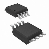
LP2966IMM-1833/NOPB National Semiconductor, LP2966IMM-1833/NOPB Datasheet - Page 12

LP2966IMM-1833/NOPB
Manufacturer Part Number
LP2966IMM-1833/NOPB
Description
IC REG DUAL ULTRA LDO 8-MSOP
Manufacturer
National Semiconductor
Datasheet
1.LP2966IMM-5050NOPB.pdf
(15 pages)
Specifications of LP2966IMM-1833/NOPB
Regulator Topology
Positive Fixed
Voltage - Output
1.8V, 3.3V
Voltage - Input
2.7 ~ 7 V
Voltage - Dropout (typical)
-, 0.135V @ 150mA
Number Of Regulators
2
Current - Output
150mA
Operating Temperature
-40°C ~ 125°C
Mounting Type
Surface Mount
Package / Case
8-MSOP, Micro8™, 8-uMAX, 8-uSOP,
Lead Free Status / RoHS Status
Lead free / RoHS Compliant
Current - Limit (min)
-
Other names
LP2966IMM-1833
LP2966IMM-1833TR
LP2966IMM-1833TR
Available stocks
Company
Part Number
Manufacturer
Quantity
Price
Company:
Part Number:
LP2966IMM-1833/NOPB
Manufacturer:
ST
Quantity:
43 000
www.national.com
Applications Information
Input Capacitor Selection
LP2966 requires a minimum input capacitance of 1µF be-
tween the input and ground pins to prevent any impedance
interactions with the supply. This capacitor should be located
very close to the input pin. This capacitor can be of any type
such as ceramic, tantalum, or aluminium. Any good quality
capacitor which has good tolerance over temperature and
frequency is recommended.
Output Capacitor Selection
The LP2966 requires a minimum of 1µF capacitance on
each output for proper operation. To insure stability, this
capacitor should maintain its ESR (equivalent series resis-
tance) in the stable region of the ESR curves (Figure 1 and
Figure 2 over the full operating temperature range of the
application. The output capacitor should have a good toler-
ance over temperature, voltage, and frequency. The output
capacitor can be increased without limit. Larger capacitance
provides better stability and noise performance. The output
capacitor should be connected very close to the Vout pin of
the IC.
LP2966 works best with Tantalum capacitors. However, the
ESR and the capcitance value of these capacitors vary a lot
with temperature, voltage, and frequency. So while using
FIGURE 1. ESR Curve for V
FIGURE 2. ESR Curve for V
2.2µF
OUT
OUT
= 5V and C
= 3.3V and C
10085011
10085012
OUT
OUT
= 2.2µF
=
12
Tantalum capacitors, it should be ensured that the ESR is
within the limits for stability over the full operating tempara-
ture range.
For output voltages greater than 2.5V, good quality ceramic
capacitors (such as the X7R series from Taiyoyuden) can
also be used with LP2966 in applications not requiring light
load operation (
it should be ensured that the capacitance value and the ESR
are within the limits for stability over the full operating tem-
perature range.
The ESRD Series Polymer Aluminium Electrolytic capacitors
from Cornell Dubilier are very stable over temperature and
frequency. The excellent capacitance and ESR tolerance of
these capacitors over voltage, temperature and frequency
make these capacitors very suitable for use with LDO regu-
lators.
Output Noise
Noise is specified in two ways-
Spot Noise or Output noise density is the RMS sum of all
noise sources, measured at the regulator output, at a spe-
cific frequency (measured with a 1Hz bandwidth). This type
of noise is usually plotted on a curve as a function of fre-
quency.
Total output Noise or Broad-band noise is the RMS sum
of spot noise over a specified bandwidth, usually several
decades of frequencies.
Attention should be paid to the units of measurement. Spot
noise is measured in units µV/
noise is measured in µV(rms).
The primary source of noise in low-dropout regulators is the
internal reference. In CMOS regulators, noise has a low
frequency component and a high frequency component,
which storngly depend on the silicon area and quiescent
current. Noise can be reduced in two ways: by increasing the
transistor area or by increasing the current drawn by the
internal reference. Increasing the area will increase the die
size and decreases the chance of fitting the die into a small
package. Increasing the current drawn by the internal refer-
ence increases the total supply current (ground pin current)
of the IC. Using an optimized trade-off of ground pin current
and die size, LP2966 achieves low noise performance with
low quiescent current in an MSOP-8 package.
Short-Circuit Foldback protection
In the presence of a short or excessive load current condi-
tion, the LP2966 uses an internal short circuit foldback
mechanism that regulates the maximum deliverable output
current. A strong negative temperature coefficient is de-
signed into the circuit to enable extremely higher peak output
current capability (in excess of 400mA per output at room
temperature, see typical curves). Thus, a system designer
using the LP2966 can achieve higher peak output current
capability in applications where the LP2966 internal junction
temperature is kept below 125˚C. Refer to the applications
section on calculating the maximum output current capability
of the LP2966 for your application.
Error Flag Operation
The LP2966 produces a logic low signal at the Error Flag pin
(ERROR) when the corresponding output drops out of regu-
lation due to low input voltage, current limiting, or thermal
limiting. This flag has a built in Hysteresis. The timing dia-
gram in Figure 3 shows the relationship between the ER-
ROR and the output voltage. In this example, the input
voltage is changed to demonstrate the functionality of the
Error Flag.
<
5mA for the 5V output option). Once again,
√
Hz or nV/
√
Hz and total output


