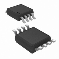
LP2966IMM-1833/NOPB National Semiconductor, LP2966IMM-1833/NOPB Datasheet - Page 5

LP2966IMM-1833/NOPB
Manufacturer Part Number
LP2966IMM-1833/NOPB
Description
IC REG DUAL ULTRA LDO 8-MSOP
Manufacturer
National Semiconductor
Datasheet
1.LP2966IMM-5050NOPB.pdf
(15 pages)
Specifications of LP2966IMM-1833/NOPB
Regulator Topology
Positive Fixed
Voltage - Output
1.8V, 3.3V
Voltage - Input
2.7 ~ 7 V
Voltage - Dropout (typical)
-, 0.135V @ 150mA
Number Of Regulators
2
Current - Output
150mA
Operating Temperature
-40°C ~ 125°C
Mounting Type
Surface Mount
Package / Case
8-MSOP, Micro8™, 8-uMAX, 8-uSOP,
Lead Free Status / RoHS Status
Lead free / RoHS Compliant
Current - Limit (min)
-
Other names
LP2966IMM-1833
LP2966IMM-1833TR
LP2966IMM-1833TR
Available stocks
Company
Part Number
Manufacturer
Quantity
Price
Company:
Part Number:
LP2966IMM-1833/NOPB
Manufacturer:
ST
Quantity:
43 000
Tsh(h)
Shutdown Input
V
T
T
I
Error Flag Comparators
V
V
V
I
I
AC Parameters
PSRR
ρn(1/f)
e
SD
EF(leak)
(EFsink)
n
Electrical Characteristics
dOFF
dON
SDT
T
TH
ERR(Sat)
Limits in standard typeface are for T
range. Unless otherwise specified, V
Note 1: Absolute maximum ratings indicate limits beyond which damage to the device may occur. Operating ratings indicate conditions for which the device is
intended to be functional, but do not guarantee specific performance limits. For guaranteed specifications and test conditions, see Electrical characteristics. The
guaranteed specifications apply only for the test conditions listed. Some performance characteristics may degrade when the device is not operated under the listed
test conditions.
Note 2: At elevated temperatures, devices must be derated based on package thermal resistance. The device in the surface-mount package must be derated at
θ
protection.
Note 3: The human body model is a 100pF capacitor discharged through a 1.5kΩ resistor into each pin.
Note 4: : Typical numbers are at 25˚C and represent the most likely parametric norm.
Note 5: : Limits are 100% production tested at 25˚C. Limits over the operating temperature range are guaranteed through correlation using Statistical Quality Control
(SQC) methods. The limits are used to calculate National’s Averaging Outgoing Quality Level (AOQL).
Note 6: If used in a dual-supply system where the regulator load is returned to a negative supply, the LP2966 output must be diode-clamped to ground.
Note 7: The output PMOS structure contains a diode between the V
will turn on this diode.
Note 8: Output voltage line regulation is defined as the change in output voltage from the nominal value due to change in input line voltage.
Note 9: Output voltage load regulation is defined as the change in output voltage from the nominal value when the load current changes from 1mA to 100mA.
Note 10: Output voltage cross regulation is defined as the percentage change in the output voltage from the nominal value at one output when the load current
changes from 1mA to full load in the other output. This is an important parameter in multiple output regulators. The specification for ∆V
specification for ∆V
Note 11: Error Flag threshold and hysteresis are specified as the percentage below the regulated output voltage.
Note 12: Dropout voltage is defined as the input to output differential at which the output voltage drops 100mV below the nominal value. Drop-out voltage
specification applies only to output voltages greater than 2.7V. For output voltages below 2.7V, the drop-out voltage is nothing but the input to output differential, since
the minimum input voltage is 2.7V.
jA
= 235˚C/W, junction-to-ambient. Please refer to the applications section on maximum current capability for further information. The device has internal thermal
Symbol
O2
/∆I
OUT1
Thermal Shutdown
Hysteresis
Shutdown Threshold
(Note 15)
Turn-off Delay (Note
17)
Turn-on Delay (Note
17)
SD Input Current
Threshold (output
goes high to low)
Threshold Hysteresis
Error Flag Saturation
Error Flag Pin
Leakage Current
Error Flag Pin Sink
Current
Ripple Rejection
Output Noise Density
Output Noise Voltage
(rms)
.
Parameter
j
IN
= 25˚C, and limits in boldface type apply over the full operating junction temperature
= V
O(NOM)
(Continued)
Output = Low
Output = High
I
I
V
V
(Note 11)
(Note 11)
I
V
120Hz, V
V
120Hz, V
f =120Hz
BW = 10Hz − 100kHz,
C
BW = 300Hz − 300kHz,
C
L
L
Fsink
SD
SD
IN
IN
OUT
OUT
= 100 mA
= 100 mA
= V
= V
= V
= 0 V
= 100µA
= 10µF
= 10µF
+ 1V, (Note 16), C
OUT
OUT
IN
Conditions
IN
OUT
OUT
and V
+ 1V, f =
+ 0.3V, f =
= 3.3V
= 3.3V
OUT
terminals that is normally reverse-biased. Reversing the polarity from V
5
OUT
= 1µF, I
Typ (Note
0.015
150
100
V
25
20
25
10
60
40
4)
0
1
1
5
1
1
1
IN
OUT
= 1mA, C
V
LP2966IMM (Note 5)
IN
Min
5
2
- 0.1
IN
= 1µF, V
O1
SD1
Max
0.1
0.1
16
/∆I
8
OUT2
= V
SD2
is equal to the
www.national.com
IN
and V
µV(rms)
= V
µV/
µsec
µsec
Unit
mA
nA
nA
dB
˚C
%
%
V
V
√
IN
OUT
Hz
.


