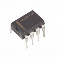
MAX688CPA Maxim Integrated Products, MAX688CPA Datasheet - Page 3

MAX688CPA
Manufacturer Part Number
MAX688CPA
Description
IC REG LINEAR LDO 3.3V FXD 8-DIP
Manufacturer
Maxim Integrated Products
Datasheet
1.MAX688CPA.pdf
(12 pages)
Specifications of MAX688CPA
Regulator Topology
Positive Fixed
Voltage - Output
3.3V
Voltage - Input
Up to 11V
Voltage - Dropout (typical)
0.04V @ 200mA
Number Of Regulators
1
Current - Output
1A
Operating Temperature
0°C ~ 70°C
Mounting Type
Through Hole
Package / Case
8-DIP (0.300", 7.62mm)
Lead Free Status / RoHS Status
Contains lead / RoHS non-compliant
Current - Limit (min)
-
Available stocks
Company
Part Number
Manufacturer
Quantity
Price
Company:
Part Number:
MAX688CPA
Manufacturer:
MAXIM
Quantity:
5 510
Company:
Part Number:
MAX688CPA
Manufacturer:
MAXIM
Quantity:
5 510
ELECTRICAL CHARACTERISTICS (continued)
(V
noted. Typical values are at T
Note 1: Minimum V
Note 2: Dropout voltage is defined as V
Note 3: The start-up time specification is the time taken from ON or SHDN rising to BASE sinking current. V
Note 4: Minimum load capacitance is a function of R
Note 5: The nominal output voltage, V
Shutdown Threshold Voltage
Below V
MAX687: ON, PFO, SHDN
PFO Threshold Voltage Below
V
PFO Hysteresis
Shutdown Threshold Voltage
PFO Output Voltage High
PFO Output Voltage Low
ON Threshold Voltage
ON Input Leakage Current
MAX688/MAX689: SHDN, PFO
PFO Threshold Voltage
PFO Hysteresis
SHDN Threshold Voltages
SHDN Hysteresis
SHDN Input Current
PFO, SHDN Transient Rejection
PFO Output Voltage Low
PFO Off Leakage Current
Output Noise Voltage
IN
NOM
= 3.8V, SHDN = V
(Note 5)
ence and comparators are functional down to the minimum voltage specified, but the output may not be in regulation.
and is a function of load capacitance, C2, and load resistance, R
ESR of C2 should be no larger than 1/100 of R
PFT
PARAMETER
IN
_______________________________________________________________________________________
for regulated V
IN
(MAX688/MAX689), R
A
= +25°C.)
V
SYMBOL
PFT
V
NOM
OUT
V
V
V
NOM
V
V
V
V
V
V
V
V
SON
SSD
SSY
e
PFT
PFT
OH
SD
OL
OL
IH
IN
- V
IL
n
, is defined under the default conditions of testing: V
depends on the characteristics of the external PNP transistor, and on the load. The refer-
- V
SD
-
OUT
Falling V
Falling V
Falling V
I
I
Output turns on
Output remains off
Falling V
parators monitor V
On, SHDN falling
Standby
Shutdown
Rising SHDN, standby on
V
Glitch immunity
I
V
10Hz ≤ f ≤ 10kHz, I
10Hz ≤ f ≤ 1MHz, I
SOURCE
SINK
SINK
B
SHDN
PFO
when V
= 0Ω, C1 = 2.2µF, C2 = 10µF, C3 = 10nF, T
= 1.2mA, V
= 1.2mA, V
L
= 11V, V
. Minimum C2 = 10µF for loads up to 100mA and 1µF/10mA for higher loads.
High-Accuracy, Low-Dropout
L
= 1.23V
. Guaranteed by design.
OUT
OUT
OUT
OUT
= 50µA, part on, V
OUT
, comparators monitor V
, comparators monitor V
, comparators monitor V
, com-
is 50mV below its value at V
SHDN
IN
IN
CONDITIONS
OUT
LOAD
LOAD
= 2.7V
= 2.7V
> 1.25V
= 200mA
= 200mA
MAX688
MAX689
L
.
IN
= 2.7V
Linear Regulators
OUT
OUT
OUT
IN
IN
= V
= 3.8V, I
NOM
A
V
= T
OUT
2.96
3.07
2.77
1.25
MIN
110
-25
1.0
1.0
20
+ 1V.
BASE
MIN
- 0.3
= 1mA, T
to T
OUT
TYP
0.06
3.13
2.85
0.06
170
100
105
0.2
70
70
66
7
7
MAX
rise time is longer
, unless otherwise
A
= T
MAX
3.19
2.89
100
0.3
0.2
1.2
0.2
0.3
25
1
MIN
to T
UNITS
µV
MAX
mV
mV
mV
mV
mV
nA
nA
µA
µs
V
V
V
V
V
V
V
RMS
3
.


