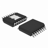
NCV8509PDW18R2G ON Semiconductor, NCV8509PDW18R2G Datasheet - Page 14

NCV8509PDW18R2G
Manufacturer Part Number
NCV8509PDW18R2G
Description
IC REG VOLT DUAL SEQ LIN 16SOIC
Manufacturer
ON Semiconductor
Datasheet
1.NCV8509PDW18R2G.pdf
(18 pages)
Specifications of NCV8509PDW18R2G
Regulator Topology
Positive Fixed
Voltage - Output
3.3V, 1.8V
Voltage - Input
Up to 50V
Voltage - Dropout (typical)
0.4V @ 100mA
Number Of Regulators
2
Current - Limit (min)
115mA, 105mA
Operating Temperature
-40°C ~ 125°C
Mounting Type
Surface Mount
Package / Case
16-SOIC (7.5mm Width) Exposed Pad, 16-eSOIC, 16-HSOIC
Polarity
Positive
Number Of Outputs
2
Output Type
Fixed
Output Voltage
1.8 V, 3.3 V
Output Current
0.115 A, 0.1 A
Line Regulation
50 mV
Load Regulation
50 mV
Dropout Voltage (max)
0.2 V
Input Voltage Max
50 V
Maximum Operating Temperature
+ 125 C
Minimum Operating Temperature
- 40 C
Mounting Style
SMD/SMT
Voltage Regulation Accuracy
2 %
Lead Free Status / RoHS Status
Lead free / RoHS Compliant
Current - Output
-
Lead Free Status / Rohs Status
Lead free / RoHS Compliant
Other names
NCV8509PDW18R2GOS
Power Dissipation
power on chip by utilizing an external resistor, R
the power on chip, P
the power dissipated in the resistor P
where
and
V
careful system validation should be performed for stability).
The voltage on V
has three modes of operation, as seen in Figure 50.
saturation voltage of the shunt output NPN.
the shunt circuit, V
since I
IN2
NCV8509 has a power shunt circuit which reduces the
P TOTAL + (V IN1 * V OUT1) I OUT1
Based on equation 3, the power in R
Mode 1. At low battery V
Mode 2. Once V
Mode 3. V
. (Increasing R
OUT2
V IN2 +
is not infinite, when V
P REX + (V IN1 * V IN2 ) I OUT2
IN2
) (V IN1 * V OUT2 ) I OUT2 ) (V IN1
P IC + P TOTAL * P REX
IN2
would continue to regulate at V
IN2
IN1
EX
IC
is controlled by the shunt circuit, which
, is equal to the total power, P
V REF
V IN1 * (I OUT2
will regulate at the V
rises above the reference voltage of
may require an increase in C
IN1
IN2
where V
SAT
is equal to V
IN1
REX
rises higher than the
. Refer to Figure 49.
EX
REF
R EX )
is dependent on
REF
= V
IN1
.
Z
minus the
EX
T
− V
REF
, minus
http://onsemi.com
for V IN1 t (V REF ) V SAT )
for (V REF ) V SAT ) t V IN1 t (V REF ) (I OUT2
for (V REF ) (I OUT2
. Thus
IN2
Iq)
, but
BE
. A
(1)
(2)
(3)
when Q1 is normally conducting.
14
reference voltage plus the voltage drop across the external
resistor R
equations for power across R
Equation 4 provides a summary for V
Combining equations 3 and 4 gives three different
R
V
I
EX
OUT2
OUT2
V
V
IN1
IN2
EX
P MODE2 + (V IN1 * V REF )
I OUT )) t V IN1
, it will force V
V
SAT
P MODE1 + (V SAT
P MODE3 + I OUT2 2
+
−
Q1
Q2
Shunt
Figure 49.
NCV8509
V
IN2
Z
EX
Circuitry
Control
to be V
.
GND
Iq
I OUT2 )
IN1
IN2.
R EX
R EX ))
− (I
I OUT2
Q3
(4)
OUT2
V
I
OUT1
OUT1
× R
EX
(5)
(6)
(7)
).


