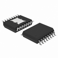
NCV8509PDW18R2G ON Semiconductor, NCV8509PDW18R2G Datasheet - Page 8

NCV8509PDW18R2G
Manufacturer Part Number
NCV8509PDW18R2G
Description
IC REG VOLT DUAL SEQ LIN 16SOIC
Manufacturer
ON Semiconductor
Datasheet
1.NCV8509PDW18R2G.pdf
(18 pages)
Specifications of NCV8509PDW18R2G
Regulator Topology
Positive Fixed
Voltage - Output
3.3V, 1.8V
Voltage - Input
Up to 50V
Voltage - Dropout (typical)
0.4V @ 100mA
Number Of Regulators
2
Current - Limit (min)
115mA, 105mA
Operating Temperature
-40°C ~ 125°C
Mounting Type
Surface Mount
Package / Case
16-SOIC (7.5mm Width) Exposed Pad, 16-eSOIC, 16-HSOIC
Polarity
Positive
Number Of Outputs
2
Output Type
Fixed
Output Voltage
1.8 V, 3.3 V
Output Current
0.115 A, 0.1 A
Line Regulation
50 mV
Load Regulation
50 mV
Dropout Voltage (max)
0.2 V
Input Voltage Max
50 V
Maximum Operating Temperature
+ 125 C
Minimum Operating Temperature
- 40 C
Mounting Style
SMD/SMT
Voltage Regulation Accuracy
2 %
Lead Free Status / RoHS Status
Lead free / RoHS Compliant
Current - Output
-
Lead Free Status / Rohs Status
Lead free / RoHS Compliant
Other names
NCV8509PDW18R2GOS
2500
2000
1500
1000
450
400
350
300
250
200
150
100
9.5
9.0
8.5
8.0
7.5
500
10
50
0
−40
0
0
0
5 V
3.3 V
2.6 V
2.5 V
1.8 V
−20
10
Figure 24. V
Figure 20. Reset Delay Time versus
Figure 22. Slew Rate versus C
25
20
3.3 V/1.8 V
0
OUTPUT CURRENT (mA)
30
TEMPERATURE (°C)
20
OUT1
Temperature
50
40
C
SLEW
Dropout Voltage
40
50
TYPICAL PERFORMANCE CHARACTERISTICS
(nF)
5 V/2.5 V
60
75
60
70
80
5 V/2.6 V
100
Slew
80
100
http://onsemi.com
90
120
125
100
8
800
700
600
500
400
300
200
100
40
35
30
25
20
15
10
16
14
12
10
5
0
0
8
6
4
2
0
0
0
30
2.5 V
3.3 V
1.8 V
5 V
Figure 21. Reset Delay Time versus C
Figure 25. Quiescent Current vs. V
20
2
40
Figure 23. Slew Rate versus C
2.6 V
4
40
50
OUTPUT CURRENT (mA)
3.3 V/1.8 V
6
60
5 V/2.6 V
5 V/2.5 V
C
60
C
Delay
8
Slew
80
(nF)
(nF)
10
70
100
I
out1
12
80
= I
120
out2
14
Slew
IN1
= 50 mA
90
Delay
140
16
160
100
18


