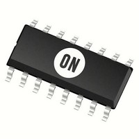
NCV8509PDW18G ON Semiconductor, NCV8509PDW18G Datasheet

NCV8509PDW18G
Specifications of NCV8509PDW18G
Related parts for NCV8509PDW18G
NCV8509PDW18G Summary of contents
Page 1
NCV8509 Series Sequenced Linear Dual-Voltage Regulator The NCV8509 Series are dual voltage regulators whose output voltages power up in such a manner as to protect the integrity of modern day microcontroller I/O and ESD input structures. Newer generation microcontrollers require ...
Page 2
MAXIMUM RATINGS V (dc) IN1 V Peak Transient Voltage IN1 V (dc) IN2 V (Current out of pin) IN2 Operating Voltage Input Voltage Range (SLEW, RESET, Delay) V OUT1 V OUT2 Electrostatic Discharge (Human Body Model) (Machine Model) Package Thermal ...
Page 3
ELECTRICAL CHARACTERISTICS mF; unless otherwise noted.) VOUT1 VOUT2 Characteristic SLEW SLEW Charging Current SLEW = 1 SLEW Rate (Note 4) C OUT1 SLEW 5 V Option 3.3 V Option V SLEW Rate C ...
Page 4
PIN DESCRIPTION Pin No. Symbol Á Á Á Á Á Á Á Á Á Á Á Á Á 1 SLEW Á Á Á Á Á Á Á Á Á Á Á Á Á Á Á Á Á Á Á Á ...
Page 5
TYPICAL PERFORMANCE CHARACTERISTICS 2.65 2.64 2.63 2.62 2.61 2.60 2.59 2.58 2.57 2.56 2.55 −40 − Temperature (°C) Figure 3. 2.6 V Output Voltage 2.55 2.54 2.53 2.52 2.51 2.50 2.49 2.48 2.47 2.46 2.45 ...
Page 6
TYPICAL PERFORMANCE CHARACTERISTICS 1.8 1.6 1.4 25°C 1.2 1.0 0.8 0.6 0.4 0 (mA) OUT1 Figure 9. I versus I Q 1.2 1.0 25°C 0.8 0.6 0.4 0 ...
Page 7
TYPICAL PERFORMANCE CHARACTERISTICS 125°C 25°C −40° (V) IN1 Figure 15 versus V OUT1 3.0 2.5 2.0 1.5 1.0 0.5 25°C −40°C 125°C ...
Page 8
TYPICAL PERFORMANCE CHARACTERISTICS 10 9.5 9.0 8.5 8.0 7.5 −40 − TEMPERATURE (°C) Figure 20. Reset Delay Time versus Temperature 2500 5 V 2000 3.3 V 1500 2.6 V 1000 2.5 V 1.8 V 500 0 ...
Page 9
TYPICAL PERFORMANCE CHARACTERISTICS 1000 3.3 V UNSTABLE REGION 100 10 1 0.1 0. OUTPUT CURRENT (mA) Figure 26. V Output Capacitor ESR (10 mF) OUT1 1000 3.3 V, 0.1 mF 100 3.3 V, ...
Page 10
TYPICAL PERFORMANCE CHARACTERISTICS (Load Transient waveforms shown were measured on the 5 V/2.6 V device) Figure 32. V Load Transient Response OUT1 100 Load & No Load to 100 mA Figure 34. V Load Transient Response OUT1 ...
Page 11
V V IN1 IN1 V V OUT1 OUT1 V V OUT2 OUT2 Figure 39. Output Decay vs. Load Impedance Max V Delta IN I(V ) × R IN2 EX 4 IN1 IN2 TIMING DIAGRAMS V IN1 V ...
Page 12
OUT1 RESET Reset Delay Power Up RESET The RESET function gets its drive from both the input (V ) and the output (V ). Because of this able to IN1 OUT1 maintain a more reliable ...
Page 13
V IN1 IN2 Voltage Regulator V OUT2 Figure 42. Power Shunt V IN1 18 V 135 Ω 100 mA V IN2 4 OUT2 2.5 V 100 mA R LOAD Figure 44. Why Use a Power ...
Page 14
Power Dissipation NCV8509 has a power shunt circuit which reduces the power on chip by utilizing an external resistor, R the power on chip equal to the total power the power dissipated in the resistor ...
Page 15
V V IN1 Mode 1 V IN1 t V REF ) V SAT V IN2 + V IN1 * V SAT 100 200 400 Copper Area (mm Figure 51. 16 Lead SOW ...
Page 16
V OUT1 ≈ 10 μs V OUT2 Disable Time Decay Time Dependent on External Load Short On V OUT1 Figure 52. Fault Response. Note the High SLEW Rate Coming Out of Fault Conditions. Soft Start Only Applies to a Power ...
Page 17
... ORDERING INFORMATION Device NCV8509PDW18G NCV8509PDW18R2G NCV8509PDW25G NCV8509PDW25R2G NCV8509PDW26G NCV8509PDW26R2G †For information on tape and reel specifications, including part orientation and tape sizes, please refer to our Tape and Reel Packaging Specifications Brochure, BRD8011/D. Output Voltage Package SOIC 16 Lead (Pb−Free) 3.3 V/1.8 V SOIC 16 Lead (Pb− ...
Page 18
... DIMENSIONS: INCHES *For additional information on our Pb−Free strategy and soldering details, please download the ON Semiconductor Soldering and Mounting Techniques Reference Manual, SOLDERRM/D. N. American Technical Support: 800−282−9855 Toll Free USA/Canada Europe, Middle East and Africa Technical Support: ...


