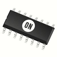
NCV8509PDW18G ON Semiconductor, NCV8509PDW18G Datasheet - Page 12

NCV8509PDW18G
Manufacturer Part Number
NCV8509PDW18G
Description
IC REG LDO DUAL 3.3/1.8V 16-SOIC
Manufacturer
ON Semiconductor
Datasheet
1.NCV8509PDW18R2G.pdf
(18 pages)
Specifications of NCV8509PDW18G
Regulator Topology
Positive Fixed
Voltage - Output
3.3V, 1.8V
Voltage - Input
Up to 50V
Voltage - Dropout (typical)
0.4V @ 100mA
Number Of Regulators
2
Current - Limit (min)
115mA, 105mA
Operating Temperature
-40°C ~ 125°C
Mounting Type
Surface Mount
Package / Case
16-SOIC (7.5mm Width) Exposed Pad, 16-eSOIC, 16-HSOIC
Polarity
Positive
Number Of Outputs
2
Output Type
Fixed
Output Voltage
1.8 V, 3.3 V
Output Current
0.115 A, 0.1 A
Line Regulation
50 mV
Load Regulation
50 mV
Dropout Voltage (max)
0.2 V
Input Voltage Max
50 V
Maximum Operating Temperature
+ 125 C
Minimum Operating Temperature
- 40 C
Mounting Style
SMD/SMT
Voltage Regulation Accuracy
2 %
Lead Free Status / RoHS Status
Lead free / RoHS Compliant
Current - Output
-
Lead Free Status / Rohs Status
Lead free / RoHS Compliant
RESET
(V
maintain a more reliable reset valid signal. Most regulators
maintain a valid reset signal down to 1 V on the output
voltage. The reset on the NCV8509 is valid down to 0 V on
the output voltage V
the reset on the NCV8509 is valid down to 0 V on the input
voltage V
Figure 41 for operation timing diagrams.
Delay Function
external capacitor) delay on the RESET output lead.
to the external delay capacitor during the following
proceedings:
The RESET function gets its drive from both the input
The reset delay circuit provides a programmable (by
The delay lead provides source current (typically 6.0 μA)
IN1
1. During power up (once the regulation threshold
2. After a reset event has occurred and the device is
) and the output (V
has been verified);
back in regulation.
IN1
(power is provided via V
OUT1
RESET
V
OUT1
OUT1
(power is provided via V
V
IN
Power Up
). Because of this, it is able to
Reset Delay
OUT1
Figure 41. Dual Drive RESET Valid
). Refer to
CIRCUIT DESCRIPTION
IN1
http://onsemi.com
Short on
V
) and
OUT1
Reset Delay
12
(RESET threshold) has been violated. This is a latched
incident. The capacitor will fully discharge and wait for the
device to regulate before going through the delay time event
again.
Power Shunt
second input pin (V
internal shunt. A simplified version of this shunt is shown in
Figure 42. This has the effect of reducing the amount of
power dissipated on chip. The effects of choosing the
external resistor value are shown in Figure 43.
using the following equation:
V
Turn Off
The delay capacitor is discharged when the regulation
R
Selection of the optimum Rex resistor value can be done
When not using the power shunt, short V
IN1
EX
Fast
routes some of the current used in the V
Reset Delay
Output Peak
RESET
IN2
(V in(max) * 4.5)
). This is accomplished by using an
I out2(max)
IN1
OUT2
to V
IN2
to a
.


