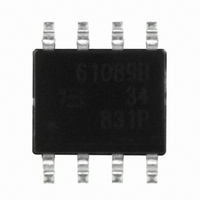
TISP61089BDR-S Bourns Inc., TISP61089BDR-S Datasheet - Page 2

TISP61089BDR-S
Manufacturer Part Number
TISP61089BDR-S
Description
SURGE PROT THYRIST 155VRING SLIC
Manufacturer
Bourns Inc.
Datasheet
1.TISP61089BDR-S.pdf
(20 pages)
Specifications of TISP61089BDR-S
Package / Case
8-SOIC (3.9mm Width)
Voltage - Breakover
*
Voltage - Off State
170V
Current - Peak Pulse (10 X 1000µs)
30A
Current - Hold (ih)
150mA
Number Of Elements
2
Capacitance
100pF
Applications
SLIC
Number Of Circuits
2
Voltage - Working
-100V
Voltage - Clamping
-112V
Technology
Mixed Technology
Breakover Current Ibo Max
6.5 A
Rated Repetitive Off-state Voltage Vdrm
170 V
Off-state Leakage Current @ Vdrm Idrm
0.005 mA
Holding Current (ih Max)
150 mA (Min)
Mounting Style
SMD/SMT
Lead Free Status / RoHS Status
Lead free / RoHS Compliant
Power (watts)
-
Lead Free Status / RoHS Status
Lead free / RoHS Compliant, Lead free / RoHS Compliant
Other names
TISP61089BDR-STR
Available stocks
Company
Part Number
Manufacturer
Quantity
Price
Company:
Part Number:
TISP61089BDR-S
Manufacturer:
LITTLEFUSE
Quantity:
4 114
Company:
Part Number:
TISP61089BDR-S
Manufacturer:
Bourns Inc.
Quantity:
31 562
Part Number:
TISP61089BDR-S
Manufacturer:
BOURNS/伯恩斯
Quantity:
20 000
Specifications are subject to change without notice.
Customers should verify actual device performance in their specific applications.
The SLIC line driver section is typically powered from 0 V (ground) and a negative voltage in the region of -20 V to -150 V. The protector gate is
connected to this negative supply. This references the protection (clipping) voltage to the negative supply voltage. The protection voltage will
then track the negative supply voltage and the overvoltage stress on the SLIC is minimized.
Positive overvoltages are clipped to ground by diode forward conduction. Negative overvoltages are initially clipped close to the SLIC negative
supply rail value. If sufficient current is available from the overvoltage, then the protector SCR will switch into a low voltage on-state condition.
As the overvoltage subsides, the high holding current of TISP61089B SCR prevents d.c. latchup.
The TISP61089B is intended to be used with a series combination of a 40 Ω or higher resistance and a suitable overcurrent protector. Power
fault compliance requires the series overcurrent element to open-circuit or become high impedance (see Applications Information). For
equipment compliant to ITU-T recommendations K.20 or K.21 or K.45 only, the series resistor value is set by the coordination requirements.
For coordination with a 400 V limit GDT, a minimum series resistor value of 10 Ω is recommended.
These monolithic protection devices are fabricated in ion-implanted planar vertical power structures for high reliability and in normal system
operation they are virtually transparent. The TISP61089B buffered gate design reduces the loading on the SLIC supply during overvoltages
caused by power cross and induction. The TISP61089B is available in a 8-pin plastic small-outline surface mount package.
OCTOBER 2000 - REVISED JULY 2008
Repetitive peak off-state voltage, V
Repetitive peak gate-cathode voltage, V
Non-repetitive peak on-state pulse current (see Notes 1 and 2)
Non-repetitive peak on-state current, 60 Hz (see Notes 1, 2 and 3)
Non-repetitive peak gate current, 1/2 µs pulse, cathodes commoned (see Notes 1 and 2)
Operating free-air temperature range
Junction temperature
Storage temperature range
NOTES: 1. Initially, the protector must be in thermal equilibrium with -40 °C ≤ T
Description (Continued)
Absolute Maximum Ratings, -40
TISP61089B High Voltage Ringing SLIC Protector
10/1000 µs (Telcordia (Bellcore) GR-1089-CORE, Issue 2, February 1999, Section 4)
5/320 µs (ITU-T K.20, K.21& K.45, K.44 open-circuit voltage wave shape 10/700 µs)
10/360 µs (Telcordia (Bellcore) GR-1089-CORE, Issue 2, February 1999, Section 4)
1.2/50 µs (Telcordia (Bellcore) GR-1089-CORE, Issue 2, February 1999, Section 4)
2/10 µs (Telcordia (Bellcore) GR-1089-CORE, Issue 2, February 1999,
Section 4)
0.5 s
1 s
2 s
5 s
30 s
900 s
2. The rated current values may be applied either to the Ring to Ground or to the Tip to Ground terminal pairs. Additionally, both
3. Values for V
to its initial conditions.
terminal pairs may have their rated current values applied simultaneously (in this case the Ground terminal current will be twice
the rated current value of an individual terminal pair). Above 85 °C, derate linearly to zero at 150 °C lead temperature.
GG
= -100 V. For values at other voltages see Figure 2.
GK
°
= 0
C
KA
≤
= 0
T J
Rating
≤
85
°
C (Unless Otherwise Noted)
J
≤ 85 °C. The surge may be repeated after the device returns
T
J
= 25 °C
Symbol
V
V
I
I
GKRM
I
GSM
T
TSM
DRM
TSP
T
T
stg
A
J
-40 to +150
-40 to +150
-40 to +85
Value
-170
-167
0.73
100
120
170
+40
6.5
4.6
3.4
2.3
1.3
30
40
40
Unit
°C
°C
°C
V
V
A
A
A


