NUP4302MR6T1G ON Semiconductor, NUP4302MR6T1G Datasheet
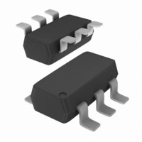
IC DIODE ARRAY SCHOTTKY TSOP6

NUP4302MR6T1G

Manufacturer Part Number
NUP4302MR6T1G
Description
IC DIODE ARRAY SCHOTTKY TSOP6
Manufacturer
ON Semiconductor
Datasheet

Specifications of NUP4302MR6T1G

Voltage - Reverse Standoff (typ)
25V
Voltage - Breakdown
30V
Power (watts)
225mW
Polarization
4 Channel Array - Bidirectional
Mounting Type
Surface Mount
Package / Case
SC-74-6
Applications
General Purpose
Number Of Circuits
4
Voltage - Working
30V
Technology
Diode Array
Product
Schottky Diodes
Peak Reverse Voltage
30 V
Forward Continuous Current
200 mA
Configuration
Octal
Recovery Time
5 ns
Forward Voltage Drop
1 V
Maximum Reverse Leakage Current
30 uA
Maximum Power Dissipation
225 mW
Operating Temperature Range
- 55 C to + 125 C
Mounting Style
SMD/SMT
Lead Free Status / RoHS Status
Lead free / RoHS Compliant
Voltage - Clamping
-
Lead Free Status / Rohs Status
Lead free / RoHS Compliant
Other names
NUP4302MR6T1G
NUP4302MR6T1GOSTR

Available stocks

Company
Part Number
Manufacturer
Quantity
Price
Part Number:
NUP4302MR6T1G
Manufacturer:
ON
Quantity:
3 000
Part Number:
NUP4302MR6T1G
Manufacturer:
ON
Quantity:
30 000
Part Number:
NUP4302MR6T1G
Manufacturer:
ON/安森美
Quantity:
20 000
Part Number:
NUP4302MR6T1G
0
NUP4302MR6
Schottky Diode Array for
Four Data Line
ESD Protection
interface from ESD, EFT and lighting.
Features
Applications
© Semiconductor Components Industries, LLC, 2006
March, 2006 − Rev. 3
The NUP4302MR6 is designed to protect high speed data line
and Class C (Exceeding 400 V) per Machine Model
Very Low Forward Voltage Drop
Fast Switching
PN Junction Guard Ring for Transient and ESD Protection
ESD Rating of Class 3B (Exceeding 16 kV) per Human Body Model
IEC 61000−4−2 Level 4 ESD Protection
Flammability Rating: UL 94 V−0
Pb−Free Package is Available
Ultra High−Speed Switching
USB 1.1 and 2.0 Power and Data Line Protection
Digital Video Interface (DVI)
Monitors and Flat Panel Displays
1
†For information on tape and reel specifications,
NUP4302MR6T1
NUP4302MR6T1G
including part orientation and tape sizes, please
refer to our Tape and Reel Packaging Specifications
Brochure, BRD8011/D.
CASE 318G
STYLE 12
Device
TSOP−6
*Date Code orientation may vary depending
(Note: Microdot may be in either location)
upon manufacturing location.
GND 2
1/O 3
I/O 1
1
ORDERING INFORMATION
67
M
G
PIN CONFIGURATION
http://onsemi.com
AND SCHEMATIC
= Specific Device Code
= Date Code
= Pb−Free Package
(Pb−Free)
Package
TSOP−6
TSOP−6
Publication Order Number:
1
MARKING
DIAGRAM
67 M G
3000/Tape & Reel
3000/Tape & Reel
NUP4302MR6/D
G
6 I/O
5 V
4 I/O
Shipping
CC

Related parts for NUP4302MR6T1G

NUP4302MR6T1G Summary of contents

Page 1

... Code orientation may vary depending upon manufacturing location. ORDERING INFORMATION Device Package NUP4302MR6T1 TSOP−6 NUP4302MR6T1G TSOP−6 (Pb−Free) †For information on tape and reel specifications, including part orientation and tape sizes, please refer to our Tape and Reel Packaging Specifications Brochure, BRD8011/D. ...

Page 2

MAXIMUM RATINGS (T = 25°C unless otherwise noted) J Rating Peak Reverse Breakdown Voltage Forward Power Dissipation (T = 25°C) A Forward Continuous Current Junction Operating Temperature Storage Temperature Range Stresses exceeding Maximum Ratings may damage the device. Maximum Ratings ...

Page 3

25°C A 85°C 100 25° 0.2 0.4 0 FORWARD VOLTAGE (VOLTS) F Figure 2. Forward Current as a Function of Forward Voltage; Typical Values ...

Page 4

... Pb−Free strategy and soldering details, please download the ON Semiconductor Soldering and Mounting Techniques Reference Manual, SOLDERRM/D. ON Semiconductor and are registered trademarks of Semiconductor Components Industries, LLC (SCILLC). SCILLC reserves the right to make changes without further notice to any products herein ...

Related keywords