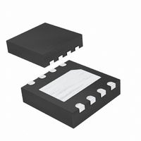
MAX6397TATA+T Maxim Integrated Products, MAX6397TATA+T Datasheet - Page 14

MAX6397TATA+T
Manufacturer Part Number
MAX6397TATA+T
Description
IC SW OVERVOLT PROT 8-TDFN
Manufacturer
Maxim Integrated Products
Datasheet
1.MAX6399ATAT.pdf
(18 pages)
Specifications of MAX6397TATA+T
Voltage - Working
72V
Technology
Mixed Technology
Power (watts)
1.45W
Number Of Circuits
1
Applications
General Purpose
Package / Case
8-TDFN Exposed Pad
Lead Free Status / RoHS Status
Lead free / RoHS Compliant
Voltage - Clamping
-
When OUT exceeds the adjusted overvoltage threshold,
an internal GATE pulldown current is enabled until OUT
drops by 5%. The capacitance at OUT is discharged by
the internal current sink and the external OUT load cur-
rent. The discharge time (∆t1) is approximately:
where V
is the external load current and I
internal 100mA (typ) pulldown current.
When OUT falls 5% below the overvoltage threshold
point, the internal current sink is disabled and the
MAX6397/MAX6398’s internal charge pump begins
recharging the external GATE voltage. The OUT volt-
age continues to drop due to the external OUT load
current until the MOSFET gate is recharged. The time
needed to recharge GATE and re-enhance the external
nFET is approximately:
where C
is the MOSFET’s gate-to-source threshold voltage, V
the internal clamp diode forward voltage (V
and I
rent (75µA typ).
Overvoltage Protection Switch/Limiter
Controllers Operate Up to 72V
Figure 12. Junction Temperature vs. C
14
______________________________________________________________________________________
GATE
OV
ISS
170
130
180
160
150
140
120
is the MAX6397/MAX6398 charge-pump cur-
is the adjusted overvoltage threshold, I
is the MOSFET’s input capacitance, V
∆t
1
1
∆t
C
I
T
GATE
OUT
A
2
=
= +125°C
= 0
= 0
=
C
C
OUTPUT CAPACITANCE (µF)
GATE
C
OUT
GATE
C
10
= InF
ISS
= ADDITIONAL CAPACITANCE
I
FROM GATE TO GND
OUT
V
V
THERMAL SHUTDOWN
GS TH
OV
C
(
I
+
GATE
GATE
100
×
GATEPD
OUT
)
I
GATEPD
= 10nF
0 05
+
.
V
F
is the GATE’s
1000
F
= 1.5V typ),
GS(TH)
OUT
F
is
During ∆t2, C
The voltage across C
MOSFET reaches its V
approximated using the following formula:
Once the MOSFET V
output voltage rise is determined by the MOSFET Q
charge through the internal charge pump with respect
to the drain potential. The time for the OUT voltage to
rise again to the overvoltage threshold can be approxi-
mated using the following formula:
where ∆V
The total period of the overvoltage waveform can be
summed up as follows:
The MAX6397/MAX6398 dissipate the most power dur-
ing an overvoltage event when I
charged only by the internal current sink). The maximum
power dissipation can be approximated using the follow-
ing equation:
The die temperature (T
(8.3°C/W and 8.5°C/W for the MAX6397 and MAX6398,
respectively) of the package when mounted correctly
with a strong thermal contact to the circuit board. The
MAX6397/MAX6398 thermal shutdown is governed by
the equation:
For the MAX6397, the power dissipation of the internal
linear regulator must be added to the overvoltage pro-
tection circuit power dissipation to calculate the die
temperature. The linear regulator power dissipation is
calculated using the following equation:
For example, using an IRFR3410 100V n-channel
MOSFET, Figure 12 illustrates the junction temperature
vs. output capacitor with I
V
100mA. Figure 12 shows the relationship between output
capacitance versus die temperature for the conditions
listed above.
OV
P
< 16V,V
DISS
(typical thermal-shutdown temperature)
T
OUT
J
= T
=
∆
F
OUT
t
= ( V
P
A
V
3
= 1.5V, I
REG
OV
+ P
t
OVP
∆
≅
loses charge through the output load.
OV
V
×
DISS
= (V
2
GS
V
= ∆t1 + ∆t2 + ∆t3
GS QGD
x 0.05) + ∆V2.
0 975
=
OUT
(
Q
.
GATE
TH
IN
GS(TH)
x (θ
_
GD
J
I
) increase is related to θ
OUT
) is obtained, the slope of the
– V
(∆V2) decreases until the
JC
×
OUT
REG
= 75mA, and I
C
I
+ θ
GATEPD
threshold and can be
×
∆
OUT
OUT
t
) (I
2
= 0, T
CA)
∆
I
GATE
V
REG
OUT
= 0 (C
< 170°C
)
×
A
∆
= +125°C,
OUT
t
GATEPD
∆
OVP
t
1
is dis-
JC
G
=


