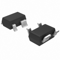
MGA-53543-TR1G Avago Technologies US Inc., MGA-53543-TR1G Datasheet - Page 7

MGA-53543-TR1G
Manufacturer Part Number
MGA-53543-TR1G
Description
IC AMP RFIC 1.9GHZ SOT-343
Manufacturer
Avago Technologies US Inc.
Datasheet
1.MGA-53543-TR1G.pdf
(14 pages)
Specifications of MGA-53543-TR1G
Gain
14dB ~ 17dB
Rf Type
Cellular, PCS
Current - Supply
40mA ~ 70mA
Frequency
0Hz ~ 2.4GHz
Noise Figure
1.5dB ~ 1.9dB
P1db
18.6dBm
Package / Case
SC-70-4, SC-82-4, SOT-323-4, SOT-343
Test Frequency
1.9GHz
Voltage - Supply
5V ~ 5.5V
Frequency Range
50MHz To 6GHz
Noise Figure Typ
1.5dB
Power Dissipation Pd
400mW
Supply Current
54mA
Supply Voltage Range
5V
Manufacturer's Type
Linear Amplifier
Number Of Channels
1
Frequency (max)
6GHz
Operating Supply Voltage (max)
5.5V
Package Type
SOT-343
Mounting
Surface Mount
Pin Count
3 +Tab
Noise Figure (typ)
1.9@2400MHzdB
Lead Free Status / RoHS Status
Lead free / RoHS Compliant
Lead Free Status / RoHS Status
Lead free / RoHS Compliant, Lead free / RoHS Compliant
Other names
516-1826-2
MGA-53543-TR1G
MGA-53543-TR1G
Available stocks
Company
Part Number
Manufacturer
Quantity
Price
Company:
Part Number:
MGA-53543-TR1G
Manufacturer:
AVAGO
Quantity:
15 600
Company:
Part Number:
MGA-53543-TR1G
Manufacturer:
AVAGO
Quantity:
11 800
Part Number:
MGA-53543-TR1G
Manufacturer:
AVAGO/安华高
Quantity:
20 000
Table 1. OIP3 vs. supply power.
Voltage
(V)
1V
V
3V
4V
5V
Matching
The most important criterion when designing with the
MGA-53543 is choosing the input and output-matching
network. The MGA-53543 is designed to give excellent IP3
performance, however to achieve this requires both the
input and output matching network to present specific
impedances (Γ
to match this part for best NF or best gain. However, this
will impact the IP3 performance. To achieve best noise
figure, the input match will need to be modified to pres-
ent gamma opt to the device. To achieve the best gain
will require both the input and output to be conjugately
matched (which will also result in the best return loss).
Where needed, the match presented to the input and
the output of the device can be modified to compromise
between IP3, NF and gain performance.
The MGA-53543 has isolation large enough to allows
input and output reflection coefficients to be replaced
by S11 and S.
In general matching for minimum noise figure does not
necessarily guarantee good IP3 performance nor does
it guarantee good gain. This is due to the fact that the
impedance parameters shown below in Table are not
guaranteed to lie near each other on a Smith Chart. So,
ideally if all input matching parameters lied near each
other or at the same point, and all output parameters also
lied near each other or at the same point, the amplifier
would have minimum Noise Figure, maximum IP3 and
maximum Gain all with a single match. Typically this is
not the case and some parameter must be sacrificed to
improve another. Table briefly lists the input and output
parameters required for each type of match while Figure 13
depicts how each is defined.
Figure 13. Definition of matching parameters.
7
Gain
50Ω
IP3
NF
Match
Input
S11*
Γ
Γ
opt
S
Γ
Γ
S11
opt
S
OIP3
(dBm)
0
17
8
35
39
S
*
*
and Γ
53
S22
Γ
L
*
L
) to the device. It is also possible
Γ
S22*
L
Output
Match
Id
(mA)
4
16
4
41
51
50Ω
Table 2. Required matching for NF, IP3, input & output Return Loss and
Gain.
Match
for
IP3
NF
RL
RL
Gain
PCB Layout
A recommended PCB pad layout for the miniature SOT-
343 (SC-70) package used by the MGA-53543 is shown
in Figure 14.
Figure 14. Recommended PCB Pad Layout for Avago’s SC70 4L/SOT-343
Products.
This layout provides ample allowance for package place-
ment by automated assembly equipment without add-
ing parasitics that could impair the high frequency RF
performance of the MGA-53543. The layout is shown with
a footprint of a SOT-343 package superimposed on the
PCB pads for reference.
A microstrip layout with sufficient ground vias as shown in
Figure 6 is recommended for the MGA-53543 in transitioning
from a package pad layout as in Figure 14.
INPUT
Figure 15. Microstripline Layout.
0.039
1.00
out
in
RF
0.024
0.60
Input
Tuning
Γ
Γ
S11*
none
S11*
53
0.045
1.15
0.051
1.30
s
opt
Dimensions in
RF
OUTPUT
Output
Tuning
Γ
none
none
S*
S*
L
inches
0.079
0.035
2.00
mm
0.9


