ADL5542ACPZ-R7 Analog Devices Inc, ADL5542ACPZ-R7 Datasheet - Page 7
ADL5542ACPZ-R7
Manufacturer Part Number
ADL5542ACPZ-R7
Description
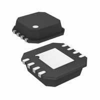
IC GAIN BLOCK 6GHZ 20DB 8LFCSP
Manufacturer
Analog Devices Inc
Datasheet
1.ADL5542ACPZ-R7.pdf
(12 pages)
Specifications of ADL5542ACPZ-R7
Gain
11.2dB ~ 14.4dB
Rf Type
Cellular, CATV
Current - Supply
93mA ~ 115mA
Frequency
50MHz ~ 6GHz
Noise Figure
5.7dB ~ 6.3dB
P1db
6.8dBm
Package / Case
8-LFCSP
Test Frequency
5.8GHz
Voltage - Supply
4.5V ~ 5.5V
Frequency Range
50MHz To 6000MHz
Noise Figure Typ
5.7dB
Power Dissipation Pd
500mW
Supply Current
92mA
Supply Voltage Range
4.5V To 5.5V
Lead Free Status / RoHS Status
Lead free / RoHS Compliant
Lead Free Status / RoHS Status
Lead free / RoHS Compliant, Lead free / RoHS Compliant
Other names
ADL5542ACPZ-R7
ADL5542ACPZ-R7TR
Q3394642A
ADL5542ACPZ-R7TR
Q3394642A
Available stocks
Company
Part Number
Manufacturer
Quantity
Price

Part Number:
ADL5542ACPZ-R7
Manufacturer:
ADI/亚德诺
Quantity:
20 000


PIN CONFIGURATION AND FUNCTION DESCRIPTIONS
Table 4. Pin Function Descriptions
Pin No.
1
2, 3, 6, 7
4
5
8
Exposed Paddle
Mnemonic
RFIN
GND
CB
VPOS
RFOUT
Description
RF Input. Requires a dc blocking capacitor.
Ground. Connect these pins to a low impedance ground plane.
Low Frequency Bypass. A 1 μF capacitor should be connected between this pin and ground.
Power Supply for Bias Controller. Connect directly to external power supply.
RF Output and Supply Voltage. DC bias is provided to this pin through an inductor that is tied to the
external power supply. RF path requires a dc blocking capacitor.
Exposed Paddle. Internally connected to GND. Solder to a low impedance ground plane.
RFIN
GND
GND
CB
Figure 2. Pin Configuration
1
2
3
4
Rev. A | Page 7 of 12
(Not to Scale)
ADL5542
TOP VIEW
PIN 1
INDICATOR
8 RFOUT
7 GND
6 GND
5 VPOS
ADL5542
Related parts for ADL5542ACPZ-R7
Image
Part Number
Description
Manufacturer
Datasheet
Request
R

Part Number:
Description:
±1.7g Dual-Axis IMEMS Accelerometer Evaluation Board
Manufacturer:
Analog Devices Inc
Datasheet:

Part Number:
Description:
Inertial Sensor Evaluation System
Manufacturer:
Analog Devices Inc
Datasheet:
Part Number:
Description:
Manufacturer:
Analog Devices Inc
Datasheet:
Part Number:
Description:
Manufacturer:
Analog Devices Inc
Datasheet:
Part Number:
Description:
Manufacturer:
Analog Devices Inc
Datasheet:
Part Number:
Description:
Manufacturer:
Analog Devices Inc
Datasheet:
Part Number:
Description:
Manufacturer:
Analog Devices Inc
Datasheet:
Part Number:
Description:
Manufacturer:
Analog Devices Inc
Datasheet:
Part Number:
Description:
Manufacturer:
Analog Devices Inc
Datasheet:
Part Number:
Description:
Manufacturer:
Analog Devices Inc
Datasheet:
Part Number:
Description:
Manufacturer:
Analog Devices Inc
Datasheet:
Part Number:
Description:
Manufacturer:
Analog Devices Inc
Datasheet:
Part Number:
Description:
Manufacturer:
Analog Devices Inc
Datasheet: