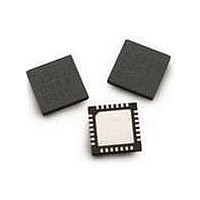
MGA-43328-BLKG Avago Technologies US Inc., MGA-43328-BLKG Datasheet

MGA-43328-BLKG
Specifications of MGA-43328-BLKG
Related parts for MGA-43328-BLKG
MGA-43328-BLKG Summary of contents
Page 1
... QFN package. It also includes shutdown and switchable gain functions. A detector is also included on-chip. The compact footprint coupled with high gain and high efficiency make the MGA-43328 an ideal choice as a power amplifier for IEEE 802.16 (WiMAX) and WLL ap- plications. ...
Page 2
Absolute Maximum Rating T =25°C A Symbol Parameter Vdd, Vbias Supply voltages, bias supply voltage Vc Control Voltage Input Power in,max [3] P Total Power Dissipation diss T Junction Temperature j,MAX T Storage Temperature STG Electrical ...
Page 3
Product Consistency Distribution Charts LSL 28 29 Figure 1. Pout_5V; LSL = 27.7dBm, Nominal = 29.3dBm LSL Figure 3. Gain; LSL = 35dB, Nominal = 37.4dB Note: 1. Distribution data sample size is 2000 samples taken from ...
Page 4
... Unless otherwise stated, all modulated signal measurements are made with IEEE 802.16e format as stated in the notes to Figure 36. MGA-43328 typical over-temperature performance at Vdd = Vbias = 5.0V 2.1V (R2 = 1.0k 390 1.1k: as shown in Figure 36), Vbyp = 0V unless otherwise stated S21 S22 -5 -10 -15 S11 -20 -25 2.0 2.1 2.2 2.3 2.4 2.5 2.6 2.7 2.8 2.9 3.0 3.1 3.2 Frequency/GHz Figure 5 ...
Page 5
... MGA-43328 typical over-temperature performance at Vdd = Vbias = 5.0V 2.1V (R2 = 1.0k 390 1.1k: as shown in Figure 36), Vbyp = 0V unless otherwise stated. 6.0 85°C 5.5 25°C 5.0 -40°C 4.5 4.0 3.5 3.0 2.5 2.0 1.5 1.0 0.5 0 Pout/dBm Figure 11. Over-temperature EVM vs Pout @ 2.7GHz 3.0 2.8 85°C 2.6 25° ...
Page 6
... MGA-43328 typical over-temperature performance at Vdd = Vbias = 5.0V 2.1V (R2 = 1.0k 390 1.1k: as shown in Figure 36), Vbyp = 0V unless otherwise stated. -25 -20 -15 - Frequency offset/MHz Figure 17. Over-temperature ETSI SEM at 29dBm Pout @ 2.5GHz -25 -20 -15 - Frequency offset/MHz Figure 19. Over-temperature ETSI SEM at 29dBm Pout @ 2.7GHz 6 ETSI 85°C 25°C -40°C ...
Page 7
... MGA-43328 typical over-temperature performance at Vdd = Vbias = 3.3V 2.1V (R2 = 1.0k 390 1.1k: as shown in Figure 36), Vbyp = 0V unless otherwise stated S22 -5 -10 -15 S11 -20 -25 1.8 1.9 2.0 2.1 2.2 2.3 2.4 2.5 2.6 2.7 2.8 2.9 3.0 Frequency/GHz Figure 20. Small-signal performance in high gain mode, Vbyp = 0V 5.0 85° ...
Page 8
... MGA-43328 typical over-temperature performance at Vdd = Vbias = 3.3V 2.1V (R2 = 1.0k 390 1.1k: as shown in Figure 36), Vbyp = 0V unless otherwise stated. 5.0 85°C 4.5 25°C 4.0 -40°C 3.5 3.0 2.5 2.0 1.5 1.0 0.5 0 Pout/dBm Figure 26. Over-temperature EVM vs Pout @ 2.7GHz 2.2 85°C 2.0 25°C 1.8 -40° ...
Page 9
... MGA-43328 typical over-temperature performance at Vdd = Vbias = 3.3V 2.1V (R2 = 1.0k 390 1.1k: as shown in Figure 36), Vbyp = 0V unless otherwise stated. -25 -20 -15 - Frequency offset/MHz Figure 32. Over-temperature ETSI SEM at 26.5dBm Pout @ 2.5GHz -25 -20 -15 - Frequency offset/MHz Figure 34. Over-temperature ETSI SEM at 26.5dBm Pout @ 2.7GHz 9 ETSI 85°C 25°C -40°C ...
Page 10
S-Parameter (Vdd = Vbias = 5.0V 2.1V Freq S11 S11 (GHz) (dB) (ang) 0.1 -5.33 174.42 0.2 -4.85 164.35 0.3 -4.70 152.36 0.4 -4.74 139.79 0.5 -5.18 126.58 0.6 -5.76 112.19 0.7 -6.56 96.27 0.8 -7.62 77.98 ...
Page 11
Freq S11 S11 (GHz) (dB) (ang) 4.1 -3.91 -143.66 4.2 -3.07 -154.67 4.3 -2.47 -164.94 4.4 -2.05 -174.00 4.5 -1.74 178.05 4.6 -1.48 171.02 4.7 -1.28 164.57 4.8 -1.12 158.68 4.9 -0.99 153.33 5.0 -0.87 148.79 5.1 -0.78 145.16 5.2 ...
Page 12
S-Parameter (Vdd = Vbias = 3.3V 2.1V Freq S11 S11 (GHz) (dB) (ang) 0.1 -5.27 173.78 0.2 -4.88 163.59 0.3 -4.74 151.80 0.4 -4.84 139.48 0.5 -5.24 126.53 0.6 -5.84 112.47 0.7 -6.60 96.97 0.8 -7.56 78.95 ...
Page 13
Freq S11 S11 (GHz) (dB) (ang) 4.1 -3.88 -142.30 4.2 -3.01 -153.64 4.3 -2.41 -164.09 4.4 -2.00 -173.45 4.5 -1.70 178.50 4.6 -1.44 171.23 4.7 -1.26 164.59 4.8 -1.10 158.61 4.9 -0.98 153.04 5.0 -0.86 148.57 5.1 -0.77 144.90 5.2 ...
Page 14
... C16 C18 C20 MGA-43228 (B) Vbyp Vc 0V (normal gain) +2.1V +5V (low gain) Pins pointing out of the page (Unit is on top Figure 35. Demonstration board application circuit for MGA-43328 module 14 Vdd3 +5V C9 C10 C11 C8 C12 RFOUT C27a C28 C27b R1 RO4350 C21 DK 3.48 C22 H 10mil W 0 ...
Page 15
Application Schematic Figure 36. Application schematic in demonstration board Notes normal gain mode operation, Vbyp = 0V. Vc1, Vc2 and Vc3 are bias pins that are used to set the bias conditions to the 3 internal gain stages ...
Page 16
PCB Land Pattern and Stencil Outline 0.300 0.250 0.250 0.600 3.600 PCB Land Pattern (Top View) 0.250 0.250 C'fer 0.300 X 45° 0.675 1.520 3.240 Combined PCB Land Pattern and Stencil Outline 16 0.250 ø 0.300 C'fer 0.300 X 45° ...
Page 17
... Ref. Bottom View Note : 1. All dimensions are in milimeters 2. Dimensions are inclusive of plating 3. Dimensions are exclusive of mold flash and metal burr. Part Number Ordering Information Part # Qty MGA-43328-BLKG 100 MGA-43328-TR1G 1000 17 0.203 Ref 0.000-0.05 0.85±0.05 Side View PIN #1 IDENTIFICATION CHAMFER 0.400 X 45° ...
Page 18
Device Orientation REEL USER FEED DIRECTION COVER TAPE Tape Dimensions 18 USER FEED DIRECTION 43328 43328 YYWW YYWW CARRIER XXXX XXXX TAPE TOP VIEW 43328 YYWW XXXX END VIEW ...
Page 19
Reel Dimensions (7” reel) SEE DETAIL "X" RECYCLE LOGO FRONT VIEW R10.65 R5.2 Slot hole ‘b’ EMBOSSED RIBS RAISED: 0.25mm, WIDTH: 1.25mm BACK VIEW For product information and a complete list of distributors, please go to our web site: Avago, ...


