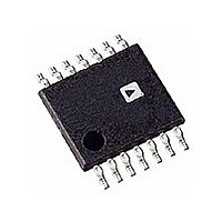
AD8302ARU-REEL Analog Devices Inc, AD8302ARU-REEL Datasheet

AD8302ARU-REEL
Specifications of AD8302ARU-REEL
Available stocks
Related parts for AD8302ARU-REEL
AD8302ARU-REEL Summary of contents
Page 1
FEATURES Measures Gain/Loss and Phase up to 2.7 GHz Dual Demodulating Log Amps and Phase Detector Input Range –60 dBm to 0 dBm Accurate Gain Measurement Scaling (30 mV/dB) Typical Nonlinearity < 0.5 dB Accurate Phase ...
Page 2
AD8302–SPECIFICATIONS resistors connected to INPA and INPB, for Phase measurement P Parameter Conditions OVERALL FUNCTION Input Frequency Range Gain Measurement Range P IN φ Phase Measurement Range IN Pin VREF, –40°C ≤ T Reference Voltage Output INPUT INTERFACE Pins INPA ...
Page 3
Parameter Conditions 900 MHz MAGNITUDE OUTPUT ± Linearity P Dynamic Range ± 0.5 dB Linearity P ± 0.2 dB Linearity P Slope From Linear Regression Deviation vs. Temperature Deviation from Output at 25°C –40°C ≤ T Deviation from ...
Page 4
... MFLT Low Pass Filter Terminal for the Magnitude Output Model AD8302ARU AD8302ARU-REEL AD8302ARU-REEL7 AD8302-EVAL CAUTION ESD (electrostatic discharge) sensitive device. Electrostatic charges as high as 4000 V readily accumulate on the human body and test equipment and can discharge without detection. Although the AD8302 features proprietary ESD protection circuitry, permanent damage may occur on devices subjected to high energy electrostatic discharges ...
Page 5
VPOS 100mV 4k INPA(INPB) 4k OFSA(OFSB) 10pF COMM Circuit A VPOS VREF 10k 5k COMM Circuit C REV 750 ON TO LOG-AMP – 2k VPOS 10k MSET (PSET) 10k ACTIVE LOADS COMM Circuit D Figure 1. Equivalent Circuits ...
Page 6
AD8302 –Typical Performance Characteristics ( the reference input and V S INPB curves, the input signal levels are equal, unless otherwise noted.) 2.0 1.8 1.6 1.4 1.2 1.0 0.8 0.6 0.4 0.2 0 –30 –25 ...
Page 7
C 1.0 0.5 0.0 –0.5 –1.0 +85 C –1.5 –40 C –2.0 –2.5 –3.0 –30 –25 –20 –15 –10 – MAGNITUDE RATIO – dB TPC 7. Distribution of Magnitude Error vs. Input Level ...
Page 8
AD8302 1.06 1.04 1. INPA INPB 1.00 0.98 0.96 0.94 0.92 0. INPA 0.88 0.86 0.84 0.82 0. 0.78 INPA INPB 0.76 0.74 0 200 400 600 800 1000 1200 1400 ...
Page 9
HORIZONTAL TPC 19. Magnitude Output Response Step, for P = –30 dBm –32 dBm to –28 dBm, Frequency INPB INPA 1900 MHz, No Filter Capacitor 20mV PER VERTICAL DIVISION 1.00 s HORIZONTAL TPC 20. ...
Page 10
AD8302 1.8 100MHz 1.6 1.4 1900MHz 1.2 2200MHz 2700MHz 1.0 0.8 0.6 0.4 0.2 0.0 –180 –140 –100 –60 –20 20 PHASE DIFFERENCE – Degrees TPC 25. Phase Output (VPHS) vs. Input Phase Difference, Input Levels –30 dBm, Frequencies 100 ...
Page 11
C – –2 +85 C –4 –6 –8 –10 –180 –150 –120 –90 –60 – PHASE DIFFERENCE – Degrees TPC 31. Distribution of VPHS Error vs. Input Phase Difference, Three ...
Page 12
AD8302 9.5 9.7 9.9 10.1 10.3 10.5 VPHS – mV/Degree TPC 37. VPHS Slope Distribution, Frequency 900 MHz 10mV PER VERTICAL DIVISION 50ns HORIZONTAL TPC 38. VPHS Output Response to 4 ...
Page 13
P = –15dBm P INPA INPA –45dBm INPA –180 –150 –120 –90 –60 –30 0 PHASE DIFFERENCE – Degrees TPC 43. Phase Output Instantaneous Slope ...
Page 14
AD8302 –2 –4 –6 –40 –30 –20 – TEMPERATURE – C TPC 49. Change in VREF vs. Temperature, Three Sigma to Either Side of Mean 120 100 ...
Page 15
GENERAL DESCRIPTION AND THEORY The AD8302 measures the magnitude ratio, defined here as gain, and phase difference between two signals. A pair of matched logarithmic amplifiers provide the measurement, and their hard-limited outputs drive the phase detector. Basic Theory Logarithmic ...
Page 16
AD8302 Note that by convention, the phase difference is taken in the range from –180° to +180°. Since this style of phase detector does not distinguish between ±90° considered to have an unambiguous 180° phase difference range that ...
Page 17
Interfacing to the Input Channels The single-ended input interfaces for both channels are identical. Each consists of a driving pin, INPA and INPB, and an ac- grounding pin, OFSA and OFSB. All four pins are internally dc-biased at about 100 ...
Page 18
AD8302 Cross Modulation of Magnitude and Phase At high frequencies, unintentional cross coupling between signals in Channels A and B inevitably occurs due to on-chip and board- level parasitics. When the two signals presented to the AD8302 inputs are at ...
Page 19
The comparator mode can be turned into a controller mode by closing the loop around the VMAG and VPHS outputs. Figure 11 illustrates a closed loop controller that stabilizes the gain and phase of a DUT with gain and phase ...
Page 20
AD8302 Reflectometer The AD8302 can be configured to measure the magnitude ratio and phase difference of signals that are incident on and reflected from a load. The vector reflection coefficient defined as, ( Γ flected ...
Page 21
AD8302 R4 COMM MFLT INPA INPA VMAG OFSA MSET VPOS VREF GND OFSB PSET INPB 6 INPB VPHS 9 C5 COMM PFLT ...
Page 22
AD8302 CHARACTERIZATION SETUPS AND METHODS The general hardware configuration used for most of the AD8302 characterization is shown in Figure 16. The characterization board is similar to the Customer Evaluation Board. Two reference-locked R and S SMT03 signal generators are ...
Page 23
Thin Shrink Small Outline Package [TSSOP] COPLANARITY REV. A OUTLINE DIMENSIONS (RU-14) Dimensions shown in millimeters 5.10 5.00 4. 4.50 6.40 4.40 BSC 4. PIN 1 0.65 BSC 1.05 1.20 1.00 MAX 0.80 0.15 0.30 ...
Page 24
Revision History Location 7/02—Data Sheet changed from REV REV. A. TPCs 3 through 6 replaced . . . . . . . . . . . . . . . . . . . . . . . ...


