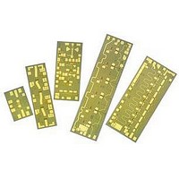
AMMC-5040-W50 Avago Technologies US Inc., AMMC-5040-W50 Datasheet - Page 2

AMMC-5040-W50
Manufacturer Part Number
AMMC-5040-W50
Description
IC MMIC AMP GAAS 20-45GHZ
Manufacturer
Avago Technologies US Inc.
Type
General Purposer
Datasheet
1.AMMC-5040-W10.pdf
(10 pages)
Specifications of AMMC-5040-W50
Function
Amplifier
Supply Current
225mA
Supply Voltage Range
2V To 5V
Frequency Max
45GHz
Frequency Min
20GHz
Supply Voltage Max
5V
Supply Voltage Min
2V
Gain
25dB
Number Of Channels
1
Frequency (max)
45GHz
Output Power
21.5@45000MHzdBm
Power Supply Requirement
Single
Single Supply Voltage (min)
2V
Single Supply Voltage (typ)
4.5V
Single Supply Voltage (max)
5V
Dual Supply Voltage (min)
Not RequiredV
Dual Supply Voltage (typ)
Not RequiredV
Dual Supply Voltage (max)
Not RequiredV
Operating Temperature Classification
Commercial
Operating Temp Range
-55C to 75C
Lead Free Status / RoHS Status
Lead free / RoHS Compliant
Lead Free Status / RoHS Status
Lead free / RoHS Compliant, Lead free / RoHS Compliant
Available stocks
Company
Part Number
Manufacturer
Quantity
Price
Part Number:
AMMC-5040-W50
Manufacturer:
AVAGO/安华高
Quantity:
20 000
Absolute Maximum Ratings
Notes:
1. Operation in excess of any one of these conditions may result in permanent damage to this device. Functional operation at or near these
2. Combinations of supply voltage, drain current, input power, and output power shall not exceed PD.
3. When operated at this condition with a base plate temperature of 85°C, the median time to failure (MTTF) is significantly reduced.
4. These ratings apply to each individual FET
5. The operating channel temperature will directly affect the device MTTF. For maximum life, it is recommended that junction temperatures be
DC Specifications/Physical Properties
Notes:
6. Measured in wafer form with T
7. Assume conductive epoxy to an evaluation RF board at 85°C base plate temperature.
Thermal Properties
2
Symbol
V
V
I
V
P
P
T
T
T
DD
Symbol
V
I
I
V
V
T
Parameters
Maximum Power Dissipation
Thermal Resistance (θjc)
Thermal Resistance (θjc)
Under RF Drive
ch
stg
max
D1
D2-3-4
d
d
g
D
in
D1,2-3-4
G1,2-3-4
P
-V
ch-b
limitations may significantly reduce the lifetime of the device.
maintained at the lowest possible levels.
g
Parameters
Drain to Gate Voltage
Positive Supply Voltage
Total Drain Current
Gate Supply Voltage
Power Dissipation
CW Input Power
Operating Channel Temp
Storage Case Temp.
Maximum Assembly Temp (30 sec max)
Parameters and Test Conditions
Drain Supply Operating Voltage
First Stage Drain Supply Current
(V
Total Drain Supply Current for Stages 2, 3 and 4
(V
Gate Supply Operating Voltages (I
Pinch-off Voltage (V
Thermal Resistance
DD
DD
= 4.5 V, V
= 4.5 V, V
G1
GG
chuck
= -0.5 V)
= -0.5 V)
[1,2,3,4, 5]
[2]
= 25°C (except T
[2,3]
[2]
[2]
DD
(Channel-to-Backside)
= 4.5 V, I
[2]
[4,5]
[6]
Test Conditions
Tbaseplate = 85°C
Vd = 4.5V
Idd = 300mA
P
Tbaseplate = 85°C
Vd = 4.5V
Idd = 306mA
Pout = 22dBm
P
Tbaseplate = 85°C
DD
D
D
ch-bs
= 1.35W
= 1.25W
< 10 mA)
DD
.)
= 300 mA)
Units
V
V
mA
V
W
dBm
°C
°C
°C
Minimum Values
-3
Units
V
mA
mA
V
V
°C/W
Value
P
Tchannel = 150°C
θjc = 31°C/W
Tchannel = 126.85°C
θjc = 31°C/W
Tchannel = 123°C
D
= 2.09W
Min.
2
Maximum Values
8
5
550
0.5
2.09
21
+150
-65 to +150
+300
Typ.
4.5
50
225
-0.45
-1.5
31
Max.
5
Notes
2
2 and 3
2
4,5


