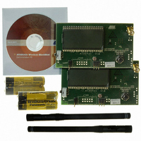
ATAB5428-8-WB Atmel, ATAB5428-8-WB Datasheet - Page 33

ATAB5428-8-WB
Manufacturer Part Number
ATAB5428-8-WB
Description
KIT DEMO 868MHZ BLACKBIRD
Manufacturer
Atmel
Series
Smart RFr
Type
Transceiver, UHFr
Specifications of ATAB5428-8-WB
Frequency
868MHz
Maximum Frequency
868 MHz
Output Power
0 dBm to 10 dBm
Supply Voltage (max)
6 V
Supply Voltage (min)
3 V
Supply Current
21 mA
Maximum Operating Temperature
+ 85 C
Board Size
2 in x 3.5 in
Minimum Operating Temperature
- 40 C
Product
RF Modules
For Use With/related Products
ATA5428
Lead Free Status / RoHS Status
Lead free / RoHS Compliant
Other names
ATAB-5428-8-WB
5.2
5.3
5.4
4841D–WIRE–10/07
AUX Mode
IDLE Mode
Reset Timing and Reset Logic
The transceiver changes from OFF mode to AUX mode if the voltage at pin VAUX V
(typically). In AUX mode DVCC and VSOUT are connected to the auxiliary power supply input
(VAUX) via the voltage regulator V_REG2. In AUX mode the transceiver is programmable via
the 4-wire serial interface, but no RX or TX operations are possible because AVCC = OFF.
The state transition OFF mode to AUX mode is indicated by an interrupt at pin IRQ and the sta-
tus bit P_On_Aux = 1.
In IDLE mode AVCC and DVCC are connected to the battery voltage (VS1).
From OFF mode the transceiver changes to IDLE mode if pin PWR_ON is set to 1 or pin T1, T2,
T3, T4 or T5 is set to “0”. This state transition is indicated by an interrupt at pin IRQ and the sta-
tus bits Power_On = 1 or ST1, ST2, ST3, ST4 or ST5 = 1.
From AUX mode the transceiver changes to IDLE mode by setting AVCC_EN = 1 in control
register 1 via the 4-wire serial interface or if pin PWR_ON is set to “1” or pin T1, T2, T3, T4 or T5
is set to “0”.
VSOUT is either connected to VS1 or to the auxiliary power supply (V_REG2).
If V
to V_REG2 and the status bit P_On_Aux is set to “1”.
In IDLE mode, the RF transceiver is disabled and the power consumption I
(VSOUT OFF and CLK output OFF and VS = VS1 = VS2 = 3V). The exact value of this current
is strongly dependent on the application and the exact operation mode, therefore check the sec-
tion
Via the 4-wire serial interface a connected microcontroller can program the required parameter
and enable the TX, RX polling or RX mode.
The transceiver can be set back to OFF mode by an OFF command via the 4-wire serial inter-
face (the bit AVCC_EN must be set to “0”, the input level of pin PWR_ON must be “0” and pin
T1, T2, T3, T4 and T5 = 1 before writing the OFF command).
Table 5-1.
If the transceiver is switched on (OFF mode to IDLE mode, OFF mode to AUX mode) DVCC and
VSOUT ramp up as illustrated in
is set to the IDLE mode). The internal signal DVCC_RESET resets the digital control logic and
sets the control register to default values.
A voltage monitor generates a low level at pin N_RESET until the voltage at pin VSOUT
exceeds 2.38V (typically) and the start-up time of the XTO has elapsed (amplitude detector, see
Figure 4-2 on page
time of the XTO has elapsed, the output clock at pin CLK is available. Because the enabling of
pin CLK is asynchronous, the first clock cycle may be incomplete.
VAUX
“Electrical Characteristics: General” on page 67
< VS1 + 0.5V, VSOUT is connected to VS1. If V
OPM1
Control Register 1
0
27). After the voltage at pin VSOUT exceeds 2.3V (typically) and the start-up
ATA5423/ATA5425/ATA5428/ATA5429
Figure 5-3 on page 34
OPM0
0
for the appropriate application case.
VAUX
(AVCC only ramps up if the transceiver
> V
S1
+ 0.5V, VSOUT is connected
S_IDLE
IDLE mode
Function
is about 230 µA
VAUX
> 3.5V
33


