RF2374PCBA-410 RFMD, RF2374PCBA-410 Datasheet - Page 4
RF2374PCBA-410
Manufacturer Part Number
RF2374PCBA-410
Description
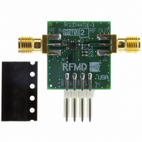
BOARD EVAL FOR RF2374
Manufacturer
RFMD
Type
Amplifierr
Datasheet
1.RF2374TR7.pdf
(13 pages)
Specifications of RF2374PCBA-410
Frequency
800MHz ~ 4GHz
For Use With/related Products
RF2374
Lead Free Status / RoHS Status
Lead free / RoHS Compliant
Other names
689-1037


RF2374
4 of 13
Gnd
Pkg
Pin
1
2
3
4
5
6
7
8
GAIN SELECT
Function
RF OUT
GND1
GND2
RF IN
VREF
GND
NC
NC
Description
RF input pin. This part is designed such that 50Ω is the optimal source
impedance for best noise figure. Best noise figure is achieved with only a
series capacitor on the input.
Ground connection. For best performance, keep traces physically short
and connect immediately to ground plane.
For low noise amplifier applications, this pin is used to control the bias cur-
rent. An external resistor can be used to set the bias current for any V
voltage. This device will have good gain and noise figure with I
3mA.
This pin selects high gain and bypass modes.
Gain Select<0.8V, high gain.
Gain Select>1.6V, low gain.
See GND1.
Amplifier output pin. This pin is an open-collector output. It must be biased
to V
Not connected.
Not connected.
This pad should be connected to the ground plane by vias directly under
the device.
7628 Thorndike Road, Greensboro, NC 27409-9421 · For sales or technical
support, contact RFMD at (+1) 336-678-5570 or sales-support@rfmd.com.
CC
through a choke or matching inductor.
Package Drawing
CC
as low as
BIAS
Interface Schematic
RF IN
To Bias
Circuit
VREF
DS101118
RF OUT
Related parts for RF2374PCBA-410
Image
Part Number
Description
Manufacturer
Datasheet
Request
R

Part Number:
Description:
3v Low Noise Amplifier Rf2374
Manufacturer:
RF Micro Devices
Datasheet:

Part Number:
Description:
IC AMP HBT GAAS CATV 8-SOIC
Manufacturer:
RFMD
Datasheet:

Part Number:
Description:
IC AMP MMIC GAAS 12GHZ 4-MICROX
Manufacturer:
RFMD
Datasheet:

Part Number:
Description:
IC AMP 3V LOW-NOISE SOT23-6
Manufacturer:
RFMD
Datasheet:

Part Number:
Description:
KIT EVAL FOR NBB-310
Manufacturer:
RFMD
Datasheet:
Part Number:
Description:
IC AMPLIFIER MMIC LNA 8-QFN
Manufacturer:
RFMD
Datasheet:
Part Number:
Description:
IC AMP MMIC GAAS 4GHZ 4-MICROX
Manufacturer:
RFMD
Datasheet:
Part Number:
Description:
IC SWITCH 10W PHEMT SPDT 12QFN
Manufacturer:
RFMD
Datasheet:
Part Number:
Description:
IC QUADRATURE MODULATOR 16-SOIC
Manufacturer:
RFMD
Datasheet:
Part Number:
Description:
100MHZ TO 4000MHZ, GAAS PHEMT MMIC LOW NOISE AMPLIFIERS
Manufacturer:
RFMD
Part Number:
Description:
KIT EVAL FOR RF2336
Manufacturer:
RFMD
Datasheet:


Part Number:
Description:
IC AMP WLAN/LNA DVR 3V SOT23-5
Manufacturer:
RFMD
Datasheet:

Part Number:
Description:
IC AMP HBT GAAS LNA BYPASS 8-QFN
Manufacturer:
RFMD
Datasheet: