AD607ARSZ-REEL Analog Devices Inc, AD607ARSZ-REEL Datasheet - Page 18

AD607ARSZ-REEL
Manufacturer Part Number
AD607ARSZ-REEL
Description
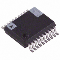
IC RECEIVER IF SUBSYS LP 20SSOP
Manufacturer
Analog Devices Inc
Datasheet
1.AD607-EBZ.pdf
(24 pages)
Specifications of AD607ARSZ-REEL
Rf Type
Cellular, GSM, CDMA, TDMA, TETRA
Function
Receiver IF Subsystem
Frequency
500MHz
Secondary Attributes
-8dBm Input Third Order Intercept
Package / Case
20-SSOP (0.200", 5.30mm Width)
Frequency Range
400kHz To 12MHz
Supply Voltage Range
2.92V To 5.5V
Rf Ic Case Style
SSOP
No. Of Pins
20
Operating Temperature Range
-40°C To +85°C
Operating Supply Voltage
3V
Operating Temperature (min)
-40C
Operating Temperature (max)
85C
Operating Temperature Classification
Industrial
Lead Free Status / RoHS Status
Lead free / RoHS Compliant
Lead Free Status / RoHS Status
Lead free / RoHS Compliant, Lead free / RoHS Compliant
AD607
Bias System
The AD607 operates from a single supply, V
a typical supply current of 8.5 mA at midgain and T = 27°C,
corresponding to a power consumption of 25 mW. Any voltage
from 2.92 V to 5.5 V may be used.
The bias system includes a fast-acting active-high CMOS-
compatible power-up switch, allowing the part to idle at 550 µA
when disabled. Biasing is proportional-to-absolute temperature
(PTAT) to ensure stable gain with temperature.
An independent regulator generates a voltage at the midpoint
of the supply (V
impedance. This voltage does not shut down, ensuring that the
major signal interfaces (e.g., mixer-to-IF and IF-to-demodulators)
remain biased at all times, thus minimizing transient disturbances
at power-up and allowing the use of substantial decoupling
capacitors on this node. The quiescent consumption of this
regulator is included in the idling current.
Figure 21. Suggested Methods for Biasing Pin FDIN at V
a. Biasing FDIN from Supply when Using
External Frequency Reference
b. Biasing FDIN from VMID when Using
External Frequency Reference
P
EXTERNAL
FREQUENCY
REFERENCE
EXTERNAL
FREQUENCY
REFERENCE
/2) that appears at the VMID pin at a low
RFHI
MAX INPUT
VPOS
54mV
50k
50k
50k
C
BYPASS
CONSTANT
( 50mV)
Figure 22. Signal Levels for Minimum and Maximum Gain
–16dBm
LOIP
FDIN
VMID
MAX OUTPUT
FDIN
AD607
AD607
1.3V
P
, usually of 3 V, at
330
MXOP
IMPEDANCE)
(TYPICAL
IF BPF
MAX INPUT
330
IFHI
54mV
(LOCATION OF OPTIONAL
P
/2
SECOND IF FILTER)
MAX OUTPUT
(VMID)
–18–
560mV
USING THE AD607
In this section, we will focus on a few areas of special impor-
tance and include a few general application tips. As is true of
any wideband high gain component, great care is needed in PC
board layout. The location of the particular grounding points
must be considered with due regard to the possibility of unwanted
signal coupling, particularly from IFOP to RFHI or IFHI or both.
The high sensitivity of the AD607 leads to the possibility that
unwanted local EM signals may have an effect on the perfor-
mance. During system development, carefully-shielded test
assemblies should be used. The best solution is to use a fully-
enclosed box enclosing all components, with the minimum
number of needed signal connectors (RF, LO, I, and Q outputs)
in miniature coax form.
The I and Q output leads can include small series resistors
(about 100 Ω) inside the shielded box without significant loss
of performance, provided the external loading during testing
is light (that is, a resistive load of more than 20 kΩ and capaci-
tances of a few picofarads). These help to keep unwanted RF
emanations out of the interior.
The power supply should be connected via a through-hole
capacitor with a ferrite bead on both inside and outside leads.
Close to the IC pins, two capacitors of different value should be
used to decouple the main supply (V
pin, VMID. Guidance on these matters is also generally included
in applications schematics.
Gain Distribution
As in all receivers, the most critical decisions in effectively using
the AD607 relate to the partitioning of gain between the various
subsections (Mixer, IF Amplifier, Demodulators) and the place-
ment of filters so as to achieve the highest overall signal-to-noise
ratio and lowest intermodulation distortion.
Figure 22 shows the main RF/IF signal path at maximum and
minimum signal levels.
IFOP
IF BPF
MAX INPUT
DMIP
154mV
Q
I
MAX OUTPUT
1.23V
IOUT
QOUT
P
) and the midpoint supply
REV. C


