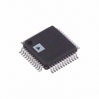
AD9874ABST Analog Devices Inc, AD9874ABST Datasheet - Page 3

AD9874ABST
Manufacturer Part Number
AD9874ABST
Description
IC IF DIGIT SUBSYSTEM 48-LQFP
Manufacturer
Analog Devices Inc
Datasheet
1.AD9874-EB.pdf
(40 pages)
Specifications of AD9874ABST
Frequency
10MHz ~ 300MHz
Rohs Status
RoHS non-compliant
Function
IF Digitizing Subsystem
Rf Type
UHF, Cellular, TETRA, GSM, EDGE, APCO25
Secondary Attributes
16dB Front End Attenuator
Package / Case
48-LQFP
Ic Function
A/D Converter (A-D)
Supply Voltage Range
2.7V To 3.6V
Operating Temperature Range
-40°C To +85°C
Digital Ic Case Style
LQFP
No. Of Pins
48
Msl
MSL 3 - 168 Hours
For Use With
AD9874-EB - BOARD EVAL FOR AD9874
Lead Free Status / RoHS Status
Lead free / RoHS Compliant
Available stocks
Company
Part Number
Manufacturer
Quantity
Price
Company:
Part Number:
AD9874ABST
Manufacturer:
AD
Quantity:
672
Part Number:
AD9874ABST
Manufacturer:
ADI/亚德诺
Quantity:
20 000
Part Number:
AD9874ABSTZ
Manufacturer:
ADI/亚德诺
Quantity:
20 000
AD9874–SPECIFICATIONS
VDDQ = VDDP = 2.7 V to 5.5 V, f
Parameter
SYSTEM DYNAMIC PERFORMANCE
LNA + MIXER
LO SYNTHESIZER
CLOCK SYNTHESIZER
SIGMA-DELTA ADC
GAIN CONTROL
OVERALL
OPERATING TEMPERATUR
NOTES
1
2
3
4
5
6
7
8
Specifications subject to change without notice.
REV. A
Standard operating mode: LNA/Mixer @ high bias setting, VGA @ Min ATTEN setting, synthesizers in normal (not fast acquire) mode, f
factor = 900, 16-bit digital output, and 10 pF load on SSI output pins.
This includes 0.9 dB loss of matching network.
AGC with DVGA enabled.
Measured in 10 kHz bandwidth.
Programmable in 0.67 mA steps.
Voltage span in which LO (or CLK) charge pump output current is maintained within 5% of nominal value of VDDP/2 (or VDDQ/2).
VDDH must be less than VDDD + 0.5 V.
Clock VCO off, add additional 0.7 mA with VGA @ Max ATTEN setting.
SSB Noise Figure @ Min VGA Attenuation
Dynamic Range with AGC Enabled
IF Input Clip Point @ Max VGA Attenuation
Input Third Order Intercept (IIP3)
Gain Variation over Temperature
Maximum RF and LO Frequency Range
LNA Input Impedance
Mixer LO Input Resistance
LO Input Frequency
LO Input Amplitude
FREF Frequency (for Sinusoidal Input ONLY)
FREF Input Amplitude
FREF Slew Rate
Minimum Charge Pump Current @ 5 V
Maximum Charge Pump Current @ 5 V
Charge Pump Output Compliance
Synthesizer Resolution
CLK Input Frequency
CLK Input Amplitude
Minimum Charge Pump Output Current
Maximum Charge Pump Output Current
Charge Pump Output Compliance
Synthesizer Resolution
Resolution
Clock Frequency (f
Center Frequency
Pass-Band Gain Variation
Alias Attenuation
Programmable Gain Step
AGC Gain Range (Continuous)
GCP Output Resistance
Analog Supply Voltage
Digital Supply Voltage
Interface Supply Voltage
Charge Pump Supply Voltage
Total Current
@ Max VGA Attenuation
@ Min VGA Attenuation
(VDDA, VDDF, VDDI)
(VDDD, VDDC, VDDL)
(VDDH)
(VDDP, VDDQ)
High Performance Setting
Low Power Mode
Standby
CLK
8
)
7
3
3, 4
8
CLK
E RANGE
= 18 MSPS, f
6
6
3, 4
2
5
5
5
5
3, 4
IF
3
= 109.65 MHz, f
(VDDI = VDDF = VDDA = VDDC = VDDL = VDDD = VDDH = 2.7 V to 3.6 V,
Temp
Full
Full
Full
Full
Full
25
25
Full
Full
Full
Full
Full
Full
Full
Full
Full
Full
Full
Full
Full
Full
Full
Full
Full
Full
Full
Full
Full
Full
Full
Full
Full
Full
Full
Full
Full
Full
Full
Full
Full
o
o
C
C
LO
= 107.4 MHz, f
–3–
Test Level Min
IV
IV
IV
IV
IV
IV
IV
IV
V
V
IV
IV
IV
IV
IV
VI
VI
VI
IV
IV
IV
VI
VI
VI
IV
IV
IV
V
IV
IV
V
V
IV
VI
VI
VI
VI
VI
VI
VI
REF
= 16.8 MHz, unless otherwise noted.)
91
–20
–32
7.75
0.3
7.5
0.48
3.87
0.4
6.25
13
0.48
3.87
0.4
16
13
50
1.8
–5
300
8
0.3
0.3
2.2
80
2.7
2.7
2.7
–40
Typ
8.1
13
95
–19
–31
0
0.7
500
370//1.4
1
0.67
5.3
0.67
5.3
f
16
12
72.5
3.0
3.0
5.0
20
17
0.01
CLK
/8
Max
9.5
2
300
2.0
25
3
0.78
6.2
VDDP – 0.4
26
VDDC
0.78
6.2
VDDQ – 0.4
24
26
1.0
95
3.6
3.6
3.6
5.5
26.5
22
0.1
+85
CLK
= 18 MHz, decimation
1
Unit
dB
dB
dB
dBm
dBm
dBm
dB
MHz
k
MHz
V p-p
MHz
V p-p
V/ s
mA
mA
V
kHz
MHz
V p-p
mA
mA
V
kHz
Bits
MHz
MHz
dB
dB
dB
dB
k
V
V
V
V
mA
mA
mA
°C
//pF


