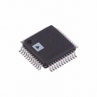
AD9874ABST Analog Devices Inc, AD9874ABST Datasheet - Page 30

AD9874ABST
Manufacturer Part Number
AD9874ABST
Description
IC IF DIGIT SUBSYSTEM 48-LQFP
Manufacturer
Analog Devices Inc
Datasheet
1.AD9874-EB.pdf
(40 pages)
Specifications of AD9874ABST
Frequency
10MHz ~ 300MHz
Rohs Status
RoHS non-compliant
Function
IF Digitizing Subsystem
Rf Type
UHF, Cellular, TETRA, GSM, EDGE, APCO25
Secondary Attributes
16dB Front End Attenuator
Package / Case
48-LQFP
Ic Function
A/D Converter (A-D)
Supply Voltage Range
2.7V To 3.6V
Operating Temperature Range
-40°C To +85°C
Digital Ic Case Style
LQFP
No. Of Pins
48
Msl
MSL 3 - 168 Hours
For Use With
AD9874-EB - BOARD EVAL FOR AD9874
Lead Free Status / RoHS Status
Lead free / RoHS Compliant
Available stocks
Company
Part Number
Manufacturer
Quantity
Price
Company:
Part Number:
AD9874ABST
Manufacturer:
AD
Quantity:
672
Part Number:
AD9874ABST
Manufacturer:
ADI/亚德诺
Quantity:
20 000
Part Number:
AD9874ABSTZ
Manufacturer:
ADI/亚德诺
Quantity:
20 000
AD9874
the maximum bandwidth is 9 kHz. A general expression for the
attack bandwidth is:
and the corresponding attack time is:
assuming that the loop dynamics are essentially those of a
single-pole system.
The 4-bit code in the AGCD field sets the ratio of the attack
time to the decay time in the amplitude estimation circuitry.
When AGCD is zero, this ratio is one. Incrementing AGCD
multiplies the decay time constant by 2
range in the decay time relative to the attack time. The decay
time may be computed from:
Figure 21a shows the AGC response to a 30 Hz pulse-modu-
lated IF burst for different AGCA and AGCD settings.
The 3-bit value in the AGCO field determines the amount of
attenuation added in response to a reset event in the ADC.
Each increment in AGCO doubles the weighting factor. At the
highest AGCO setting, the attenuation will change from 0 dB to
12 dB in approximately 10 µs, while at the lowest setting the
attenuation will change from 0 dB to 12 dB in approximately
1.2 ms. Both times assume f
the AGC attack time response for different AGCO settings.
t
t
BW
attack
decay
Figure 21a. AGC Response for Different AGCA
and AGCD Settings with f
f
CLKOUT
16
16
32
16
32
32
48
80
64
48
80
64
48
96
80
64
A
96
96
0
0
0
=
0
=
=
50
= 20 kSPS, Decimate by 900, and AGCO = 0
t
2 2 100
attack
.
×
AGCD = 8
(
f
10
CLK
× (
AGCD = 0
AGCD = 8
AGCD = 0
2
×
18
AGCD
π
CLK
MHz
×
20
AGCA = 0
AGCA = 8
AGCA = 4
2
2
TIME – ms
)
(
= 18 MHz. Figure 21b shows
AGCD = 0
AGCA
)
× (
CLK
2
2
30
)
= 18 MSPS,
1/2
AGCA
=
AGCD = 8
, allowing a 180:1
0 35
2
.
)
Hz
40
BW
A
50
(10)
(8)
(9)
–30–
Lastly, the AGCF bit reduces the DAC source resistance by at
least a factor of 10. This facilitates fast acquisition by lowering
the RC time constant that is formed with the external capacitors
connected from the GCP pin-to-ground (GCN pin). For an
overshoot-free step response in the AGC loop, the capacitor
connected from the GCP pin to the GCN ground pin should be
chosen so that the RC time constant is less than one quarter of
the raw loop. Specifically:
where R is the resistance between the GCP pin and ground
(72.5 k
the raw loop bandwidth. Note that with C chosen at this upper
limit, the loop bandwidth increases by approximately 30%.
Now consider the case described above but with the DVGA
enabled to minimize the effects of 16-bit truncation. With the
DVGA enabled, a control loop based on the larger of the two
estimated signal levels (i.e., output of DEC1 and DVGA) is
used to control the DVGA gain. The DVGA multiplies the
output of the decimation filter by a factor of 1 to 4 (i.e., 0 dB to
12 dB). When signals are small, the DVGA gain is 4 and the
16-bit output is extracted from the 24-bit data produced by the
decimation filter by dropping 2 MSB and taking the next 16
bits. As signals get larger, the DVGA gain decreases to the point
where the DVGA gain is 1 and the 16-bit output data is simply
the 16 MSB of the internal 24-bit data. As signals get even
larger, attenuation is accomplished by the normal method of
increasing the ADC’s full scale.
The extra 12 dB of gain range provided by the DVGA reduces
the input-referred truncation noise by 12 dB and makes the data
more tolerant of LSB corruption within the DSP. The price
paid for this extension to the gain range is that the start of AGC
action is 12 dB lower and that the AGC loop will be unstable if its
bandwidth is set too wide. The latter difficulty results from the
large delay of the decimation filters, DEC2 and DEC3, when
one implements a large decimation factor. As a result, given an
option, the use of 24-bit data is preferable to using the DVGA.
RC
Figure 21b. AGC Response for Different AGCO
Settings with f
Decimate by 60, and AGCA = AGCD = 0
128
112
64
96
80
48
32
16
< 1 8 (
0
0
30% if AGCF = 0, < 8 k if AGCF = 1) and BW is
0.1
π
BW
AGCO = 7
0.2
)
AGCD = 0
CLK
AGCO = 4
0.3
= 18 MSPS, f
0.4
TIME – ms
0.5
0.6
CLKOUT
0.7
= 300 kSPS,
0.8
0.9
REV. A
1.0
(11)


