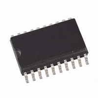
T5744N-TKS Atmel, T5744N-TKS Datasheet - Page 9

T5744N-TKS
Manufacturer Part Number
T5744N-TKS
Description
IC RCVR PLL ASK 450MHZ 20-SSOP
Manufacturer
Atmel
Datasheet
1.T5744N-TK.pdf
(19 pages)
Specifications of T5744N-TKS
Frequency
300MHz ~ 450MHz
Sensitivity
-108dBm
Modulation Or Protocol
ASK
Applications
General Purpose Data Transmission Systems
Current - Receiving
30mA
Data Interface
PCB, Surface Mount
Antenna Connector
PCB, Surface Mount
Voltage - Supply
4.5 V ~ 5.5 V
Operating Temperature
-40°C ~ 105°C
Package / Case
20-SSOP
Lead Free Status / RoHS Status
Contains lead / RoHS non-compliant
Features
-
Memory Size
-
Data Rate - Maximum
-
Pin ENABLE
4521B–RKE–01/03
Pin MODE can now be set in accordance with the desired clock cycle T
the following application-relevant parameters:
Timing of the analog and digital signal processing
IF filter center frequency (f
Most applications are dominated by two transmission frequencies: f
mainly used in USA, f
dependent parameters, the electrical characteristics display three conditions for each
parameter.
•
•
•
The clock cycle of some function blocks depends on the selected baud rate range
(BR_Range) which is defined by the Pins BR_0 and BR_1. This clock cycle T
defined by the following formulas for further reference:
BR_Range = BR_Range0:
Via the Pin ENABLE the operating mode of the receiver can be selected (see Figure 10
and Figure 11).
If the Pin ENABLE is held to Low, the receiver remains in sleep mode. All circuits for sig-
nal processing are disabled and only the XTO is running in that case. The current
consumption is I
to a transmitter signal.
To activate the receiver, the Pin ENABLE must be held to High. During the start-up
period, T
start-up period depends on the selected baud-rate range (BR_Range).
After the start-up period, all circuits are in a stable condition and the receiver is in the
receiving mode.
In receiving mode, the internal data signal (Dem_out) is switched to Pin DATA. To avoid
incorrect timing at the begin of the data stream, the begin is synchronized to a falling
edge of the incoming data signal. The receiver stays in the receiving mode until it is
switched back to sleep mode via Pin ENABLE.
During start-up and receiving mode, the current consumption is I
Application USA
(f
Application Europe
(f
Other applications
(T
characteristic is given as a function of T
XTO
XTO
Clk
Startup
is dependent on f
= 4.90625 MHz, MODE = L, T
= 6.76438 MHz, MODE = H, T
, all signal processing circuits are enabled and settled. The duration of the
BR_Range1:
BR_Range2:
BR_Range3:
S
= I
Soff
Send
in that case. During the sleep mode the receiver is not sensitive
= 433.92 MHz in Europe. In order to ease the usage of all T
IF0
XTO
)
and on the logical state of Pin MODE. The electrical
T
T
T
T
XClk
XClk
XClk
XClk
= 8 ´ T
= 4 ´ T
= 2 ´ T
= 1 ´ T
Clk
Clk
= 2.0383 µs)
= 2.0697 µs)
Clk
Clk
Clk
Clk
Clk
).
S
= I
Son
Send
.
Clk
= 315 MHz is
. T
T5744
Clk
controls
XClk
Clk
is
9
-


