MICRF500BLQTR Micrel Inc, MICRF500BLQTR Datasheet
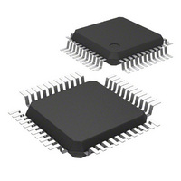
TXRX UHF 700-1100MHZ 44-LQFP

MICRF500BLQTR

Manufacturer Part Number
MICRF500BLQTR
Description
TXRX UHF 700-1100MHZ 44-LQFP
Manufacturer
Micrel Inc
Datasheet

Specifications of MICRF500BLQTR

Frequency
700MHz Center
Data Rate - Maximum
128kBaud
Modulation Or Protocol
FSK
Applications
Remote Control, Remote Metering
Power - Output
10dBm
Sensitivity
-104dBm
Voltage - Supply
2.5 V ~ 3.4 V
Current - Receiving
12mA
Current - Transmitting
50mA
Data Interface
PCB, Surface Mount
Antenna Connector
PCB, Surface Mount
Operating Temperature
-40°C ~ 85°C
Package / Case
44-LQFP
Lead Free Status / RoHS Status
Contains lead / RoHS non-compliant
Memory Size
-
General Description
The MICRF500 is a single chip UHF transceiver designed for
spread spectrum communication (FHSS) intended for ISM
(Industrial, Scientific and Medical) and SRD (Short Range
Device) frequency bands from 700MHz to 1100MHz with
FSK data rates up to 128k baud.
The transmitter consists of a PLL frequency synthesizer and
a power amplifier. The frequency synthesizer consists of a
voltage-controlled oscillator (VCO), a crystal oscillator, dual-
modulus prescaler, programmable frequency dividers and a
phase-detector. The loop filter is external for flexibility and
can be a simple passive circuit. The VCO is a Colpitts
oscillator which requires an external resonator and varactor.
FSK modulation can be applied externally to the VCO. The
synthesizer has two different N, M and A frequency dividers.
FSK modulation can also be implemented by switching
between these dividers (max. 2400bps). The lengths of the N
and M and A registers are 12, 10 and 6 bits respectively. For
all types of FSK modulation, data is entered at the DATAIXO
pin (see application circuit). The output power of the power
amplifier can be programmed to eight levels. A lock detect
circuit detects when the PLL is in lock.
In receive mode the PLL synthesizer generates the local
oscillator (LO) signal. The N, M and A values that give the LO
frequency are stored in the N0, M0 and A0 registers. The
receiver is a zero intermediate frequency (IF) type in order to
make channel filtering possible with low-power integrated
low-pass filters. The receiver consists of a low-noise amplifier
(LNA) that drives a quadrature mixer pair. The mixer outputs
feed two identical signal channels in phase quadrature. Each
channel includes a preamplifier, a third order Sallen-Key RC
low pass filter that protects the following gyrator filter from
strong adjacent channel signals and finally, a limiter. The
main channel filter is a gyrator capacitor implementation of a
seven-pole elliptic low pass filter. The elliptic filter minimizes
the total capacitance required for a given selectivity and
dynamic range. The cut-off frequency of the Sallen-Key RC
filter can be programmed to four different frequencies: 10kHz,
30kHz, 60kHz and 200kHz. An external resistor adjusts the
cut-off frequency of the gyrator filter. The demodulator de-
modulates the I and Q channel outputs and produces a digital
data output. It detects the relative phase of the I and the Q
channel signal. If the I channel signal lags the Q channel, the
FSK tone frequency lies above the LO frequency (data ‘1’). If
the I channel leads the Q channel, the FSK tone lies below the
LO frequency (data ‘0’). The output of the receiver is available
on the DATAIXO pin. A RSSI (Receive Signal Strength
Indicator) circuit indicates the received signal level.
RadioWire is a trademark of Micrel, Inc.
March 2003
MICRF500
Micrel, Inc. • 1849 Fortune Drive • San Jose, CA 95131 • USA • tel + 1 (408) 944-0800 • fax + 1 (408) 944-0970 • http://www.micrel.com
1
A two pin serial interface is used to program the circuit.
External components are necessary for RF input and output
impedance matching and decoupling of power. Other exter-
nal components are the VCO resonator circuit with varactor,
crystal, feedback capacitors and components for FSK modu-
lation with the VCO, loop filter, bias resistors for the power
amplifier and gyrator filters. A T/R switch can be implemented
with 2-pin diodes. This gives maximum input sensitivity and
transmit output power.
Features
• Frequency range: 700MHz to 1100MHz
• Modulation: FSK
• RF output power: 10dBm
• Sensitivity (19.2k bauds, BER=10
• Maximum data rate: 128k bauds
Applications
• Telemetry
• Remote metering
• Wireless controller
• Wireless data repeaters
• Remote control systems
• Wireless modem
• Wireless security system
Ordering Information
700MHz to 1.1GHz RadioWire™ RF Transceiver
Part Number
MICRF500BLQ
Ambient Temp. Range
MICRF500
–40°C to +85°C
Final
-3
): –104dBm
44-Lead LQFP
RadioWire™
Package
MICRF500
Micrel

Related parts for MICRF500BLQTR

MICRF500BLQTR Summary of contents

Page 1

MICRF500 General Description The MICRF500 is a single chip UHF transceiver designed for spread spectrum communication (FHSS) intended for ISM (Industrial, Scientific and Medical) and SRD (Short Range Device) frequency bands from 700MHz to 1100MHz with FSK data rates up ...

Page 2

MICRF500 Pin Configuration ICHOUT QCHOUT OSCVDD OSCGND CMPOUT Pin Description Pin Number Pin Name 1 IFGND 2 IFVDD 3 ICHOUT 4 QCHOUT 5 OSCVDD 6 OSCIN 7 OSCGND 8 GND 9 CMPOUT 10 CMPR 11 MOD 12 XOSCIN 13 XOSCOUT ...

Page 3

MICRF500 Pin Description, cont’t Pin Number Pin Name 24 PA_C 25 PABIAS 26 RFOUT 27 RFGND 28 RFVDD 29 RFIN 30 RFGND2 31 LNA_C 32 MIXERGND 33 MIXERVDD 34 MIXIOUTP 35 MIXIOUTN 36 IFIINP 37 IFIINN 38 MIXQOUTP 39 MIXQOUTN ...

Page 4

MICRF500 Absolute Maximum Ratings Maximum Supply Voltage (V ) ................................... +7V DD Maximum NPN Reverse Base-Emitter Voltage .......... +2.5V Storage Temperature Range (T ) ............ –55°C to +150°C S ESD Rating, Note 3 .................................................... 500V Electrical Characteristics F = 850MHz, ...

Page 5

MICRF500 Parameter Condition Receive Section f IN Receiver Sensitivity (Note 6) BER=10 Input 1dB Compression Level Input IP3 Input Impedance RSSI Dynamic Range RSSI Output Voltage Adjacent Channel Rejection 10kHz 25kHz channel spacing C ...

Page 6

MICRF500 Functional Diagram MICRF500 LNA PA 90° Prescaler 64/65 N-counter Filters S I Gyrator Filters LD ...

Page 7

MICRF500 Typical Application Figure 2 shows an example of a transceiver with modulation applied to the VCO. The VCO and matching components are optimized for 915MHz, 120kbps data rate. The inductors and trimming capacitors must have a good high frequency ...

Page 8

MICRF500 List of components Component Values R1 30Ω R2 0Ω R3 39Ω R4 10Ω R5 62Ω R6 1kΩ R7 20kΩ R8 39kΩ R9 16kΩ R10 16kΩ R11 100kΩ R12 6.8kΩ R13 270kΩ R14 2.2kΩ R16 2.2kΩ C1 47pF C4 47pF ...

Page 9

MICRF500 Applications Information VCO and PLL Section The frequency synthesizer consists of a VCO, crystal oscilla- tor, dual-modulus prescaler, programmable frequency divid- ers, phase-detector, charge pump, lock detector and an external loop filter. The dual-modulus prescaler divides the VCO-frequency by ...

Page 10

MICRF500 The bit setting that corresponds to lock can vary, depending on temperature, loop filter and type of varactor. Therefore, the lock detect circuit needs to be calibrated regularly by a software routine that finds the correct bit setting, by ...

Page 11

MICRF500 The component values will be: R101 33k IN C116 22n C115 1n R109 10k Figure 5. Third Order Loop Filter With this loop filter, internal modulation up to 2400bps is possible. The PLL lock time from power-down to Rx ...

Page 12

MICRF500 Transmit Power Amplifier (PA) The power amplifier is biased in class AB. The last stage has an open collector, and an external load inductor (L2) is therefore necessary. The DC current in the amplifier is adjusted with an external ...

Page 13

MICRF500 Bias Resistor (kΩ) Cut-Off Frequency (kHz) 2.2 6.8 8 The gyrator filter cut-off frequency should be chosen to be approximately the same as the cut-off frequency of the Sallen-Key filter. The maximum cut-off frequency of the ...

Page 14

MICRF500 Programming A two-line bus is used to program the circuit; the two lines being CLKIN and REGIN. The 2-line serial bus interface allows control over the frequency dividers and the selective powering up of Tx, Rx and Synthesizer circuit ...

Page 15

MICRF500 Name Description A1 frequency divider A1, 6 bits A0 frequency divider A0, 6 bits N1 frequency divider N1, 12 bits N0 frequency divider N0, 12 bits M1 frequency divider M1, 10 bits M0 frequency divider M0, 10 bits RxFilt ...

Page 16

MICRF500 When FSK modulation is applied to the VCO the PLL is using the dividers A1, N1 and M1. When Mod1 = 1 and Mod0 = possible to switch between the different dividers in the PLL. DATAIXO ...

Page 17

MICRF500 Example 869.0MHz 10.00MHz. FSK modula tion is applied to the VCO 135 135 RxFilt Pa2 Pa1 ...

Page 18

MICRF500 Package Information MICREL, INC. 1849 FORTUNE DRIVE SAN JOSE, CA 95131 USA + 1 (408) 944-0800 TEL The information furnished by Micrel in this datasheet is believed to be accurate and reliable. However, no responsibility is assumed by Micrel ...

Related keywords