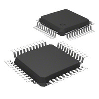
MICRF500BLQTR Micrel Inc, MICRF500BLQTR Datasheet - Page 16

MICRF500BLQTR
Manufacturer Part Number
MICRF500BLQTR
Description
TXRX UHF 700-1100MHZ 44-LQFP
Manufacturer
Micrel Inc
Datasheet
1.MICRF500EVAL1.pdf
(18 pages)
Specifications of MICRF500BLQTR
Frequency
700MHz Center
Data Rate - Maximum
128kBaud
Modulation Or Protocol
FSK
Applications
Remote Control, Remote Metering
Power - Output
10dBm
Sensitivity
-104dBm
Voltage - Supply
2.5 V ~ 3.4 V
Current - Receiving
12mA
Current - Transmitting
50mA
Data Interface
PCB, Surface Mount
Antenna Connector
PCB, Surface Mount
Operating Temperature
-40°C ~ 85°C
Package / Case
44-LQFP
Lead Free Status / RoHS Status
Contains lead / RoHS non-compliant
Memory Size
-
MICRF500
When FSK modulation is applied to the VCO the PLL is using
the dividers A1, N1 and M1. When Mod1 = 1 and Mod0 = 0
it is possible to switch between the different dividers in the
PLL. DATAIXO controls the switching. When DATAIXO = 0
the PLL uses dividers A0, N0 and M0. When DATAIXO = 1 the
PLL uses dividers A1, N1 and M1. Switching between the
different dividers can be used to implement FSK modulation.
The N, M and A values can be calculated from the formula:
where f
The 80bit control word is first read into a shift-register, and is
then loaded into a parallel register by a transition of the
REGIN signal (positive or negative) when the CLKIN signal is
high. The circuit then goes directly into the specified mode
(receive, transmit, etc.).
1. The second last bit is clocked into the first shift register
2. The last bit is clocked into the first shift register (‘1’).
3. A transition on the REGIN signal generates an internal
4. When the clock signal goes low, the power amplifier
5. The power amplifier is fully turned on.
MICRF500
Figure 10. Timing of CLKIN, REGIN and the Internal
(‘1’).
load pulse that loads the control word into the parallel
register. The circuit enters the new mode (in this case
Tx-mode). The circuit stabilizes in the new mode.
(PA) is turned on slowly in order to minimize spurious
components on the RF output signal. To be sure the
PLL is in lock before the PA is turned on, the PA should
be turned on after LOCKDET has been set.
The negative transition on the clock signal should come
a minimum time of one period of the comparison fre-
quency after the internal load pulse is generated.
LOAD_INT
LOCKDET
f
C
REGIN
C
CLKIN
PA_C
=
is the comparison frequency.
f
XCO
M
LOAD_INT and PA_C Signals
1
=
64 N A
× +
2 3
f
RF
4
5
6
7
16
6. A new control word is entered into the first register. A
7. When the power amplifier is turned off an internal load
As long as transitions on REGIN are avoided when CLKIN is
high, a new control word can be clocked into the first register
any time without affecting the operation of the transceiver.
Example 1. f
f
ing between dividers.
Binary form: (MSB to the left):
Tx:
Rx:
When FSK modulation is implemented by switching between
the different dividers A, N and M values corresponding to the
receive frequency and both transmit frequencies have to be
found.
XCO
transition on the REGIN signal when CLKIN is high will
now turn the power amplifier off.
pulse is generated. The new control word is loaded into
the parallel register and the circuit enters a new mode
(in this case power down mode). CLKIN must go low
after the internal load pulse is generated.
Rx
Rx
Rx
Rx
Rx
Tx
Tx
Tx
Tx
Tx
= 10.00MHz. FSK modulation is implemented by switch-
001001 011011 000010001001
000010000110 0001100101 0001100011
011110000000001010001011
110010 110010 000010000111
000010000111 0001100100 0001100100
01011110000000001010001001
OutS1
RxFilt
Ref6
Ref0
A1
50
9
0
0
0
0
0
0
0
0
RF
= 869.0MHz, frequency deviation: ≈ ±10kHz,
Cpmp1 Cpmp0
OutS0
Ref5
Pa2
A0
27
50
1
1
0
0
1
1
0
0
Mod1
Ref4
Pa1
137
135
N1
1
1
0
0
0
0
1
1
Mod0
Ref3
Pa0
134
135
Fc1
N0
1
1
0
0
0
0
0
0
Ref2
101
100
Fc0
M1
Gc
RT
1
1
0
0
1
1
1
0
March 2003
ByLNA
OutS2
Ref1
100
M0
99
Pu
Micrel
0
0
0
0
0
0
1
1


