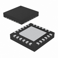
ATA8743-PXQW Atmel, ATA8743-PXQW Datasheet - Page 8

ATA8743-PXQW
Manufacturer Part Number
ATA8743-PXQW
Description
MCU W/TRANSMITTER ASK/FSK 24QFN
Manufacturer
Atmel
Datasheet
1.ATA8743-PXQW.pdf
(238 pages)
Specifications of ATA8743-PXQW
Frequency
868MHz ~ 928MHz
Applications
Home Automation, Remote Sensing, RKE
Modulation Or Protocol
ASK, FSK
Data Rate - Maximum
32 kBit/s
Power - Output
3.5dBm ~ 8dBm
Current - Transmitting
9.3mA
Data Interface
PCB, Surface Mount
Antenna Connector
PCB, Surface Mount
Memory Size
4kB Flash, 256B EEPROM, 256B SRAM
Voltage - Supply
1.8 V ~ 3.6 V
Operating Temperature
-40°C ~ 85°C
Package / Case
24-VQFN Exposed Pad, 24-HVQFN, 24-SQFN, 24-DHVQFN
Processor Series
ATA8x
Core
AVR8
Data Bus Width
8 bit
Program Memory Type
Flash
Program Memory Size
4 KB
Data Ram Size
256 B
Interface Type
SPI, USI
Maximum Clock Frequency
16 MHz
Number Of Programmable I/os
12
Number Of Timers
2
Maximum Operating Temperature
+ 85 C
Mounting Style
SMD/SMT
Development Tools By Supplier
ATASTK512-EK1-IND
Minimum Operating Temperature
- 40 C
On-chip Adc
10 bit, 8 Channel
Lead Free Status / RoHS Status
Lead free / RoHS Compliant
Features
-
Lead Free Status / Rohs Status
Details
- Current page: 8 of 238
- Download datasheet (4Mb)
3.1
3.2
3.3
8
Description of RF Transmitter
ASK Transmission
FSK Transmission
ATA8743
The integrated PLL transmitter is particularly suited to simple, low-cost applications. The VCO is
locked to 64
14.2969 MHz crystal for a 915 MHz transmitter. All other PLL and VCO peripheral elements are
integrated.
The XTO is a series resonance oscillator so that only one capacitor together with a crystal con-
nected in series to GND are needed as external elements.
The crystal oscillator together with the PLL typically need < 1 ms until the PLL is locked and the
CLK output is stable. There is a wait time of
microcontroller and the PA is switched on.
The power amplifier is an open-collector output delivering a current pulse, which is nearly inde-
pendent from the load impedance. Thus, the delivered output power is controllable via the
connected load impedance.
This output configuration enables a simple matching to any kind of antenna or to 50 . This
results in a high power efficiency of = P
868.3 MHz when an optimized load impedance of Z
voltage.
The RF TX block is activated by ENABLE = H. PA_ENABLE must remain L for t
CLK signal is taken to clock the AVR and the output power can be modulated by means of pin
PA_ENABLE. After transmission, PA_ENABLE is switched to L and the microcontroller switches
back to internal clocking. The RF TX is switched back to standby mode with ENABLE = L.
The RF TX is activated by ENABLE = H. PA_ENABLE must remain L for t
signal is taken to clock the AVR and the power amplifier is switched on with PA_ENABLE = H.
The chip is then ready for FSK modulation. The AVR starts to switch on and off the capacitor
between the XTAL load capacitor and GND with an open-drain output port, thus changing the
reference frequency of the PLL. If the switch is closed, the output frequency is lower than if the
switch is open. After transmission PA_ENABLE is switched to L and the microcontroller switches
back to internal clocking. The RF TX is switched back to standby mode with ENABLE = L.
The accuracy of the frequency deviation with XTAL pulling method is about ±25% when the fol-
lowing tolerances are considered.
Figure 3-1.
Tolerances of the Frequency Modulation
f
XTAL
XTAL
V
hence a 13.5672 MHz crystal is needed for a 868.3 MHz transmitter and a
S
C
Stray1
Crystal equivalent circuit
C
M
L
C
out
M
0
/(I
4 ms must be used until the CLK is used for the
S,PA
R
S
Load
V
S
= (166 + j226) is used at 3V supply
) of 24% for the power amplifier at
C
Stray2
C
5
C
Switch
C
4
4 ms, then the CLK
9152B–INDCO–02/10
4 ms, then the
Related parts for ATA8743-PXQW
Image
Part Number
Description
Manufacturer
Datasheet
Request
R

Part Number:
Description:
Manufacturer:
ATMEL Corporation
Datasheet:

Part Number:
Description:
DEV KIT FOR AVR/AVR32
Manufacturer:
Atmel
Datasheet:

Part Number:
Description:
INTERVAL AND WIPE/WASH WIPER CONTROL IC WITH DELAY
Manufacturer:
ATMEL Corporation
Datasheet:

Part Number:
Description:
Low-Voltage Voice-Switched IC for Hands-Free Operation
Manufacturer:
ATMEL Corporation
Datasheet:

Part Number:
Description:
MONOLITHIC INTEGRATED FEATUREPHONE CIRCUIT
Manufacturer:
ATMEL Corporation
Datasheet:

Part Number:
Description:
AM-FM Receiver IC U4255BM-M
Manufacturer:
ATMEL Corporation
Datasheet:

Part Number:
Description:
Monolithic Integrated Feature Phone Circuit
Manufacturer:
ATMEL Corporation
Datasheet:

Part Number:
Description:
Multistandard Video-IF and Quasi Parallel Sound Processing
Manufacturer:
ATMEL Corporation
Datasheet:

Part Number:
Description:
High-performance EE PLD
Manufacturer:
ATMEL Corporation
Datasheet:

Part Number:
Description:
8-bit Flash Microcontroller
Manufacturer:
ATMEL Corporation
Datasheet:

Part Number:
Description:
2-Wire Serial EEPROM
Manufacturer:
ATMEL Corporation
Datasheet:


